Touch panel and method for producing the same

a technology of resistive film and touch panel, which is applied in the direction of mechanical pattern conversion, instruments, computing, etc., can solve the problems of large size of the entire touch panel, difficult to avoid degradation of precision in detecting a touch point, and cracking of transparent conductive film on the transparent resin film

Inactive Publication Date: 2005-06-30
FUJITSU COMPONENENT LTD
View PDF6 Cites 20 Cited by
  • Summary
  • Abstract
  • Description
  • Claims
  • Application Information

AI Technical Summary

Problems solved by technology

However, if the stylus or the like is repeatedly used to press a certain point or write something, the transparent conductive film on the transparent resin film may crack.
This makes it hard to avoid degradation of precision in detecting a touched point.
This poses a problem in that the size of the entire touch panel becomes large.
This causes a reduction in the effective area of an entire touch panel.
The increase in the thickness becomes an obstacle to incorporation of the touch panel in a display device.
In the resistive-film-type touch panels with diodes according to the related arts, as diodes, each formed as a single component, are employed, after the diodes are mounted, the touch panels become bulky.
Moreover, soldering or any other work required in order to couple the diodes to respective electrodes formed on a transparent resistive film is time-consuming.
Consequently, the process of producing the touch panel becomes complex, and the cost of manufacture is hard to reduce.

Method used


Image

  • Touch panel and method for producing the same
  • Touch panel and method for producing the same
  • Touch panel and method for producing the same

Examples


Embodiment Construction

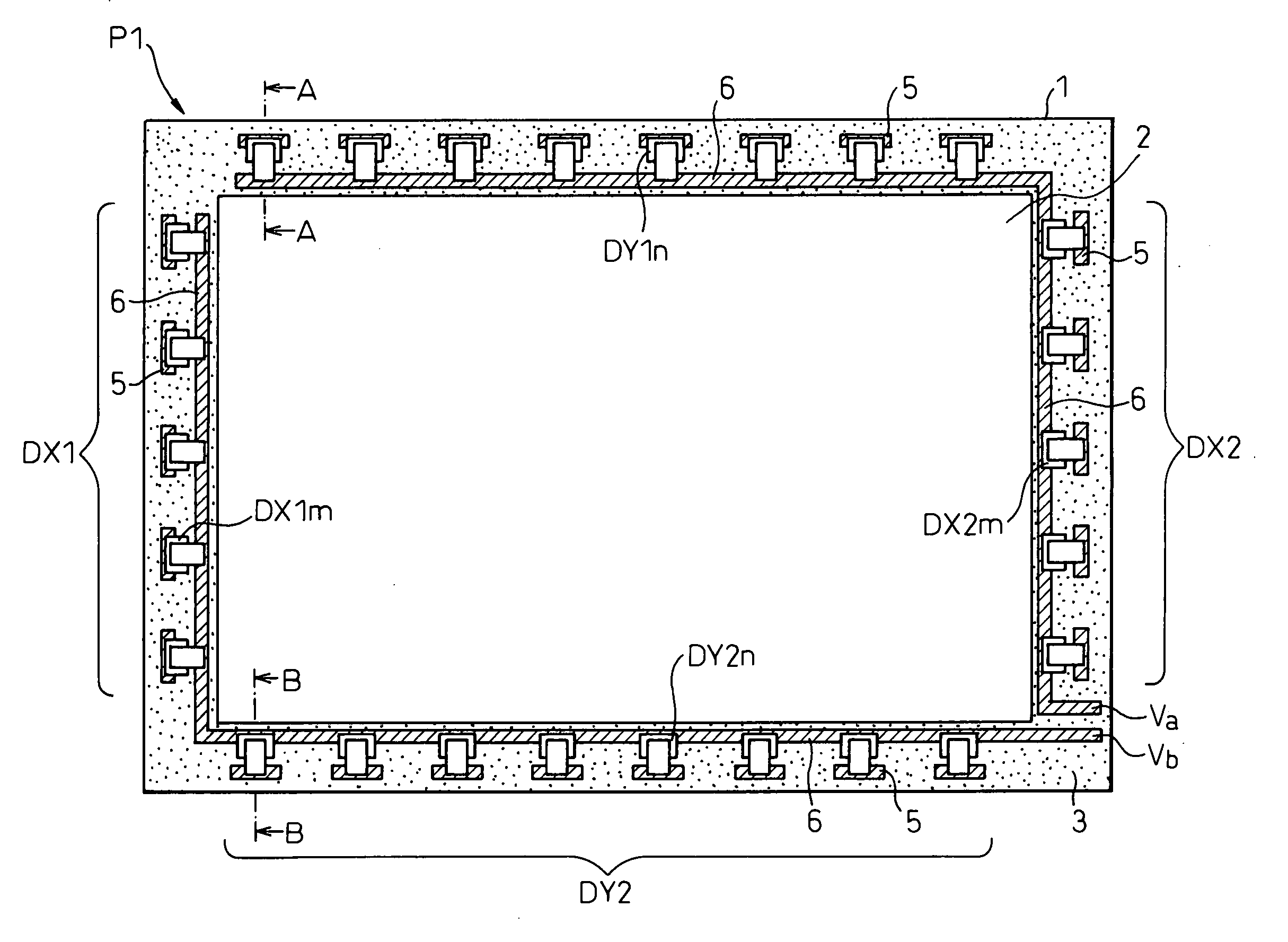
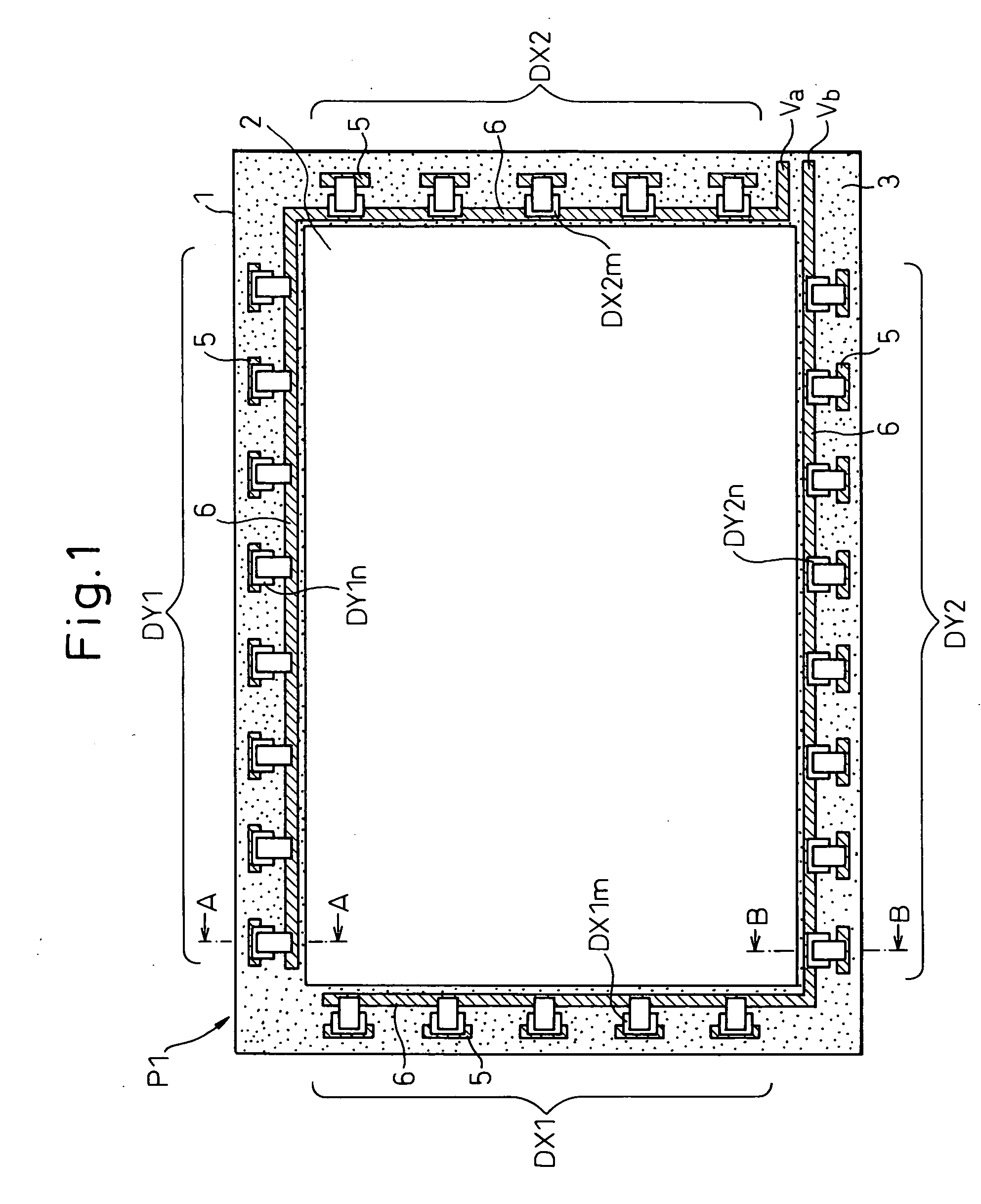
[0057] Referring to the drawings, a resistive-film type touch panel and a touch panel producing method in accordance with one embodiment of the present invention will be described below. To begin with, prior to the description of a resistive-film type touch panel and a method of producing a touch panel in accordance with the present embodiment, the structures of resistive-film type touch panels in accordance with related arts which are the fundamentals of the present embodiment will be described in order to clarify the features and advantages of the present embodiment.

[0058]FIG. 12 shows the structure of a resistive-film type touch panel in accordance with a related art, wherein diodes are adopted as switching devices. For brevity, the plan view schematically and illustratively shows the structure of the touch panel P. Note that the shape and dimensions of an actual touch panel are not presented.

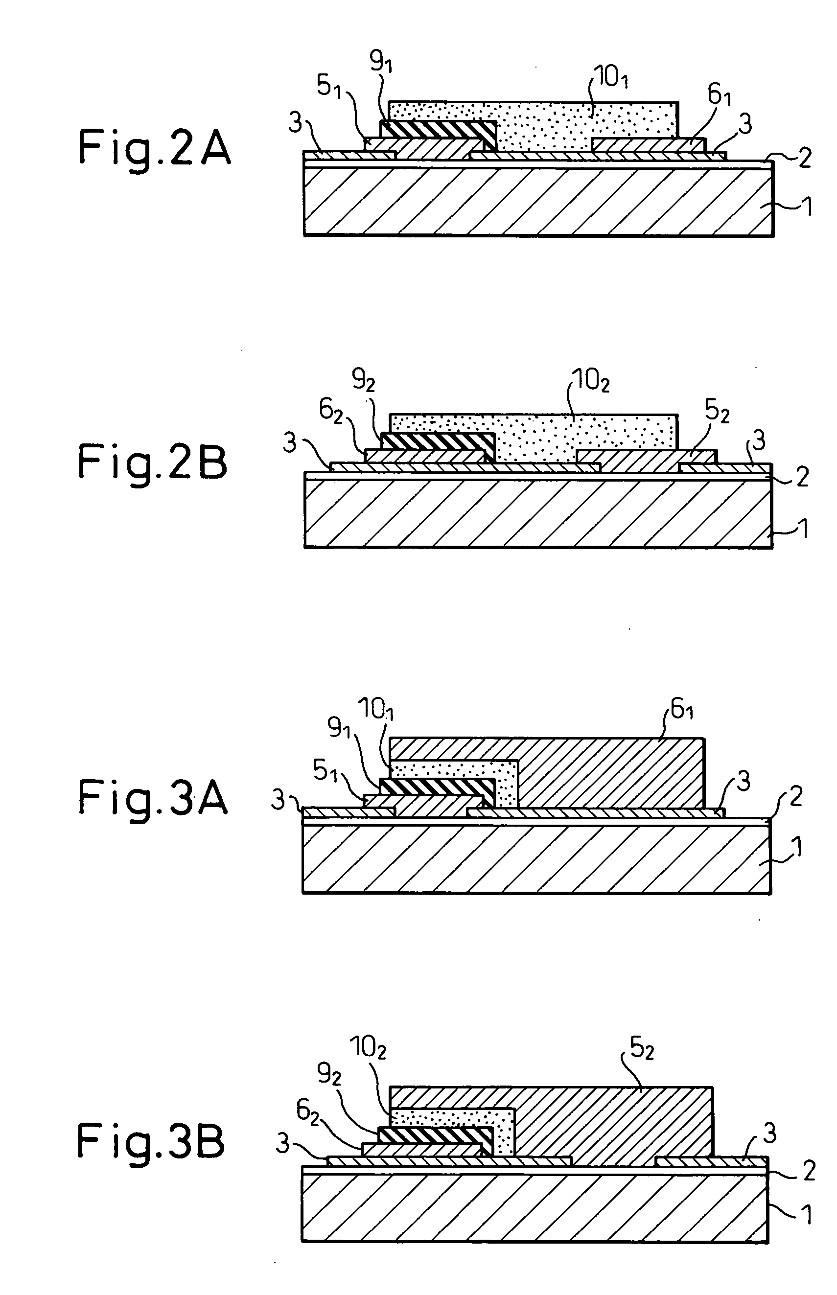
[0059] A rectangular transparent film 2 is attached to the surface of a glass substrat...


PUM


Abstract

The present invention relates to a resistive-film-type touch panel with diodes, the touch panel being reduced in thickness, in the area for arranging the diodes, and in the height thereof. An insulating film having a predetermined thickness is formed around the resistive film which is transparent and mounted on a glass substrate facing a voltage detecting electrode film. A plurality of diodes DX1m, DX2m, DY1n and DY2n, each including a semiconductor layer produced by a screen printing or stamping printing, are disposed at a predetermined pitch and connected to first electrodes electrically connected to the transparent resistive film and second electrodes for supplying voltage. A voltage gradient is formed, in the X direction and Y direction, on the transparent resistive film when a voltage is applied to each of the diodes.

Description

CROSS-REFERENCE TO RELATED APPLICATION [0001] This application claims the priority of Japanese Patent Application Number 2003-435504 filed on Dec. 26, 2003. BACKGROUND OF THE INVENTION [0002] 1. Field of the Invention [0003] The present invention relates to a resistive-film-type touch panel with switching devices and to a method for producing the touch panel. More particularly, the present invention is concerned with a touch panel and a touch panel producing method capable of guaranteeing superb durability against handwriting and a long service life, simplifying incorporation of switching devices, and reducing the thickness of a panel itself. [0004] 2. Description of the Related Art [0005] Conventionally, display devices, including liquid crystal displays, often have touch panels mounted on the display screens thereof. The inclusion of a touch panel makes it possible to directly command a computer by pressing or touching an icon or the like displayed on the display screen using a st...

Claims


Application Information

Patent Timeline
Patent Type & Authority Applications(United States)
IPC IPC(8): G06F3/045G06F3/03G06F3/041G06K11/06G08C21/00
CPCG06F3/045
Inventor ENDO, MICHIKO
Owner FUJITSU COMPONENENT LTD
Why Eureka
Try Eureka