Organic electroluminescence device

a technology of electroluminescence and organic light, which is applied in the direction of organic semiconductor devices, discharge tube luminescnet screens, natural mineral layered products, etc., can solve the problems of difficult to form pinhole-free thin films less than 1000, limited method for precisely fabricating shadow masks, and high reproduction of red (r), green (g) and blue pixels. , to achieve the effect of high color purity

Active Publication Date: 2005-06-30
LG DISPLAY CO LTD
View PDF4 Cites 132 Cited by
  • Summary
  • Abstract
  • Description
  • Claims
  • Application Information

AI Technical Summary

Benefits of technology

[0015] An object of the present invention is to provide a dual panel type organic EL device that is capable of obtaining a high color purity by forming an organic EL layer in a stack structure including a charge generation layer, an electrode transporting layer, a hole transporting layer, and an emission layer including red (R), green (G) and blue (B) emission materials, so that the dual panel type organic EL device can exhibit full colors using a color conversion medium (CCM) / color filter or a color filter.

Problems solved by technology

The related art organic EL device has a limitation in fine-patterning the red (R), green (G) and blue pixels with high reproduction under a large area.
However, this method is limited in precisely fabricating the shadow mask to have fine patterns over a resolution of a predetermined level and employing the shadow mask in a high definition and large area due to the tension deviation of the shadow mask and the like.
Also, another pixel patterning method using a high molecular organic EL material inkjet injection head has been researched, but it is difficult for forming a pinhole-free thin film less than 1000 Å.
Thus, a yield of the organic EL display is determined by both of a yield of the array device and a yield of the organic EL diode, and therefore, an overall process yield is greatly limited to a latter process, namely, the process of forming the organic EL diode.
For example, even though the array device is formed excellently, if defects occur due to foreign matters or other factors in forming the organic EL layer employing a thin film of about 1000 Å thick, the entire organic EL device is rendered defective.
Consequently, a defective organic EL layer results in decreased production yield and increased material costs in manufacturing the non-defective array element associated with the defective organic EL layer.

Method used


Image

  • Organic electroluminescence device
  • Organic electroluminescence device
  • Organic electroluminescence device

Examples


Embodiment Construction

[0025] Reference will now be made in detail to the preferred embodiments of the present invention, examples of which are illustrated in the accompanying drawings.

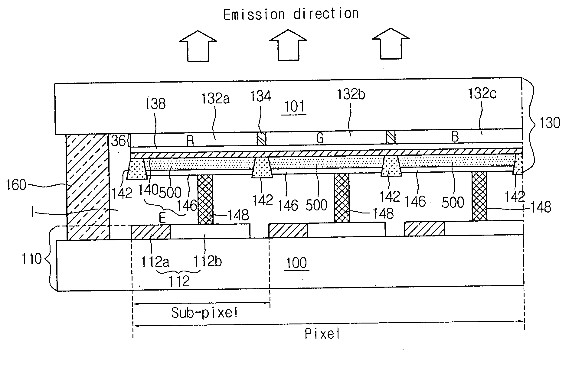
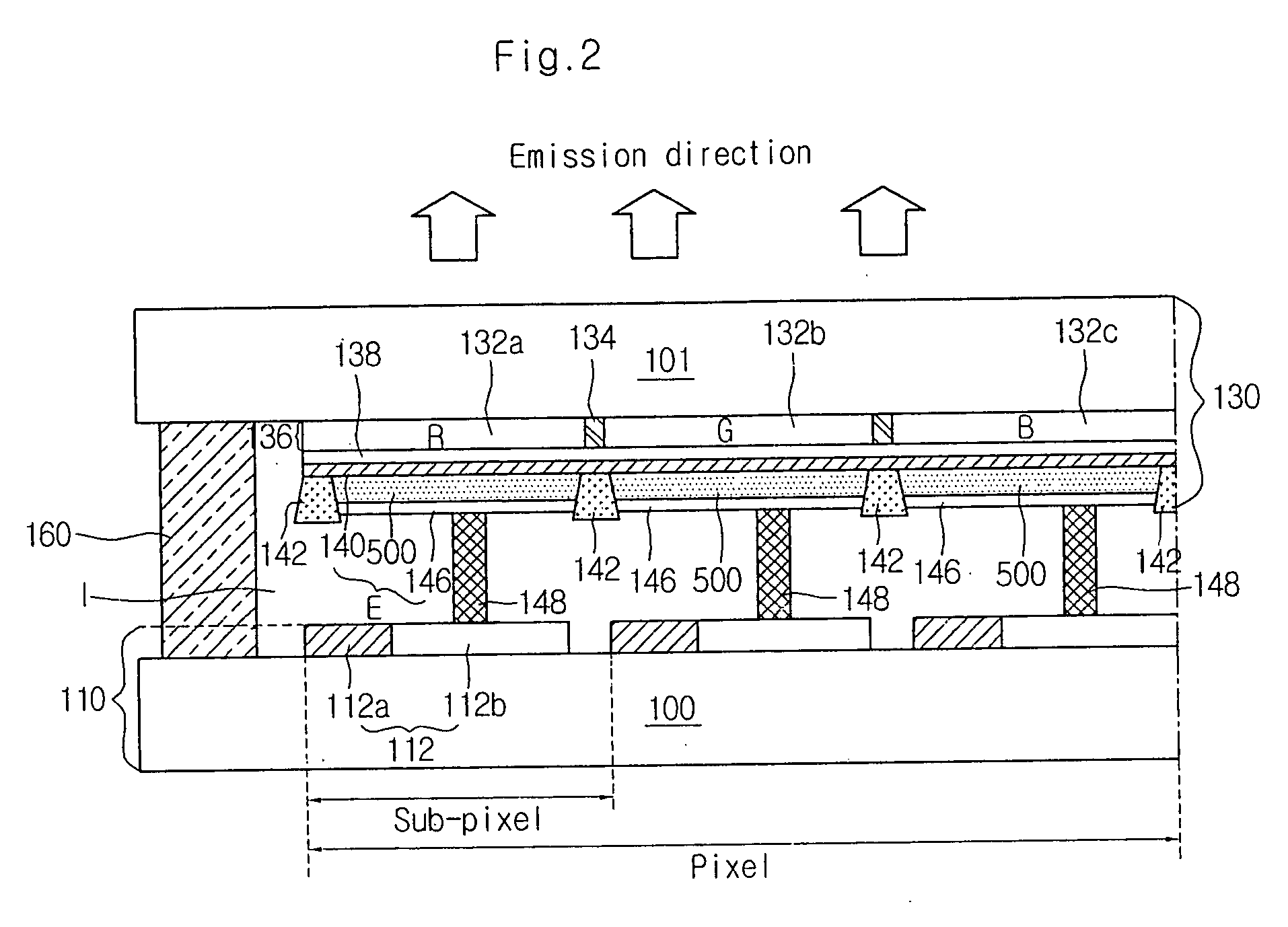
[0026]FIG. 2 is a cross-sectional view schematically showing a dual panel type organic EL device that exhibits colors in a color conversion medium (CCM) according to an exemplary embodiment of the present invention. The dual panel type organic EL device is capable of overcoming the drawbacks of the related art bottom emission type organic EL device. As shown in FIG. 2, the dual panel type organic EL device includes a first substrate 110 and a second substrate 130 disposed facing each other and attached by a seal pattern 160.

[0027] The first substrate 110 includes a transparent substrate 100 and an array element 112 formed on the transparent substrate 100. The second substrate 130 includes a transparent substrate 101, and a color conversion portion 136. The color conversion portion 136 including red (R), green (G) and blue...


PUM

PropertyMeasurementUnit
electroluminescenceaaaaaaaaaa
colorsaaaaaaaaaa
transparentaaaaaaaaaa

Abstract

An organic electronluminescence device includes an array element divided into sub-pixels and including thin film transistors formed in the sub-pixels; a color conversion portion disposed below a second substrate and including a red (R), green (G) and blue (B) conversion layer for converting white light into three primary colors of red (R), green (G) and blue (B); a first electrode disposed below the color conversion portion and including a transparent conductive material; an organic EL layer disposed below the first electrode in the sub-pixels and including a plurality of stack units each including a charge generation layer, an electrode transporting layer, a hole transporting layer and an emission layer; a second electrode patterned below the organic EL layer in the sub-pixels; and a conductive spacer electrically connecting the thin film transistors with the second electrode.

Description

[0001] The present invention claims the benefit of the Korean Application No. 99398 / 2003 filed on in Korea Dec. 29, 2003, which is hereby incorporated by reference. BACKGROUND OF THE INVENTION [0002] 1. Field of the Invention [0003] The present invention relates to a light emitting device, and more particularly, to an organic electroluminescence (EL) device. [0004] 2. Discussion of the Related Art [0005] Among flat panel displays, an organic electroluminescence (EL) device is a self-emission type display with higher contrast and wider viewing angle as compared to a liquid crystal display (LCD). The organic EL device can be made lightweight and slim profile as compared to other display types because it does not require a backlight. The organic EL device also uses less power than other types of flat panel displays. Further, the organic EL device can be driven with a low DC voltage and still have a rapid response rate. Since all of the components of the organic EL device are formed of ...

Claims


Application Information

Patent Timeline
Patent Type & Authority Applications(United States)
IPC IPC(8): H01L27/32H05B33/14H01L51/50H01L51/52H05B33/20H05B33/22H05B33/26H05B44/00
CPCH01L27/3209H01L27/322H01L27/3246H01L2251/5315H01L51/5036H01L51/5284H01L27/3251H10K59/32H10K59/127H10K59/38H10K59/122H10K50/125H10K50/865H10K2102/3026H05B33/14
Inventor PARK, JAE YONG
Owner LG DISPLAY CO LTD
Why Eureka
Try Eureka