Light emitting display, display panel, and driving method thereof

a technology of light-emitting display and display panel, which is applied in the direction of identification means, instruments, static indicating devices, etc., can solve the problems of voltage drop on the line for supplying the power supply voltage vsub>dd /sub>, further problems, and image quality degradation

Active Publication Date: 2005-06-30
SAMSUNG DISPLAY CO LTD
View PDF32 Cites 115 Cited by
  • Summary
  • Abstract
  • Description
  • Claims
  • Application Information

AI Technical Summary

Benefits of technology

[0013] In exemplary embodiments of the present invention, a current that flows to the OLED of a pixel circuit in a light emitting display is substantially prevented from being influenced by a power supply voltage.
[0014] Further, a current that flows to the OLED of a pixel circuit in a light emitting display may be substantially prevented from being influenced by deviations of a threshold voltage of a driving transistor.

Problems solved by technology

However, when a voltage drop (IR-drop) is generated on a line for supplying the power supply voltage VDD, and the power supply voltage VDD applied to a plurality of pixel circuits is not uniform, a desired amount of current may not flow to the OLED, thereby degrading image qualities, since the current flowing to the OLED is influenced by the power supply voltage VDD in the conventional pixel circuit based on the voltage programming method.
As the area of the organic EL display becomes larger, and the brightness increases, the voltage drop on the line for supplying the power supply voltage VDD increases to generate further problems.

Method used


Image

  • Light emitting display, display panel, and driving method thereof
  • Light emitting display, display panel, and driving method thereof
  • Light emitting display, display panel, and driving method thereof

Examples


Embodiment Construction

[0042] In the following detailed description, only certain exemplary embodiments of the present invention are shown and described, by way of illustration. As those skilled in the art would recognize, the described exemplary embodiments may be modified in various different ways, all without departing from the spirit or the scope of the invention. Accordingly, the drawings and description are to be regarded as illustrative in nature, and not restrictive.

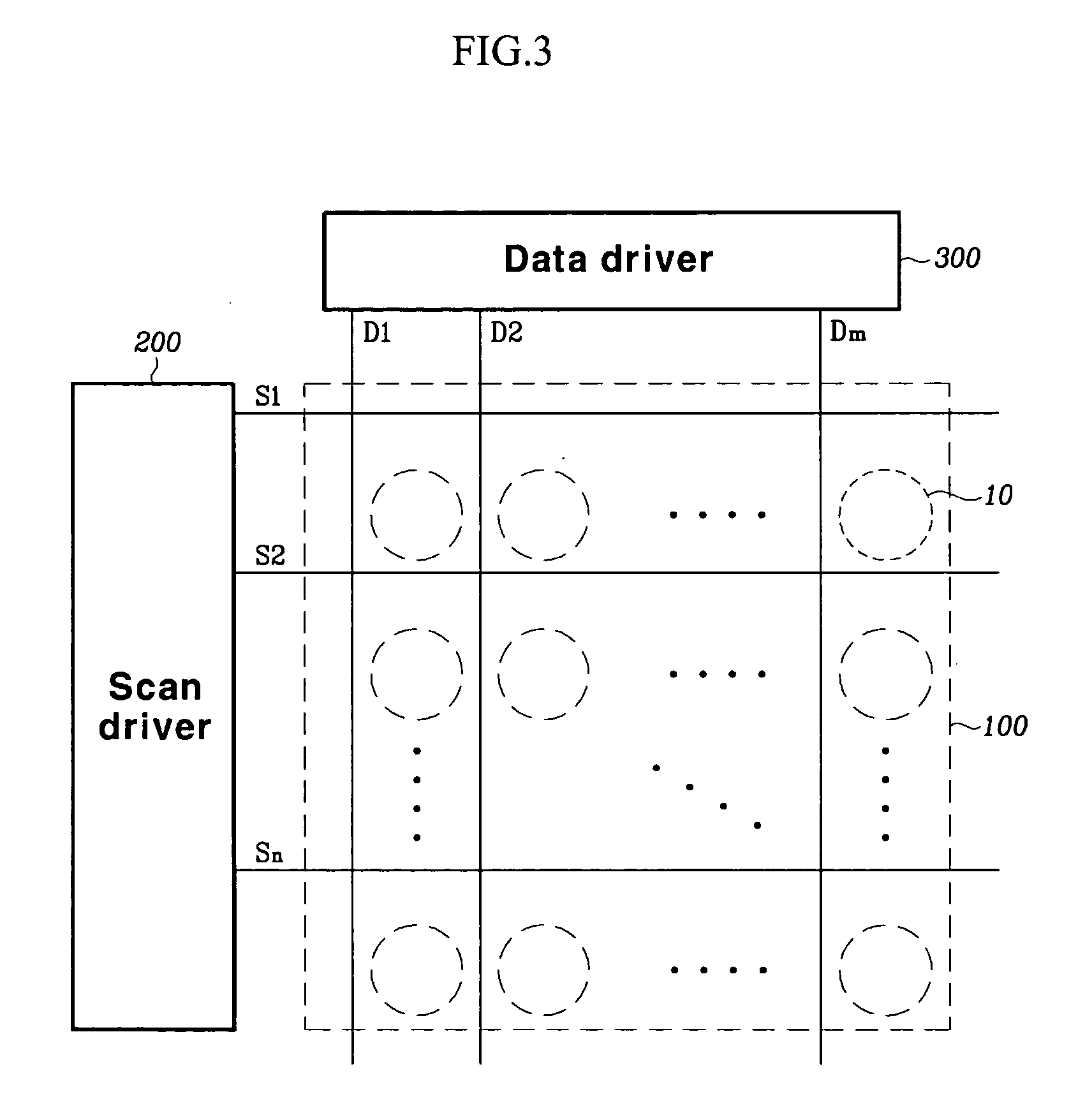
[0043]FIG. 3 shows an organic EL display according to an exemplary embodiment of the present invention.

[0044] As shown, the organic EL display includes an organic EL display panel 100, a scan driver 200, and a data driver 300.

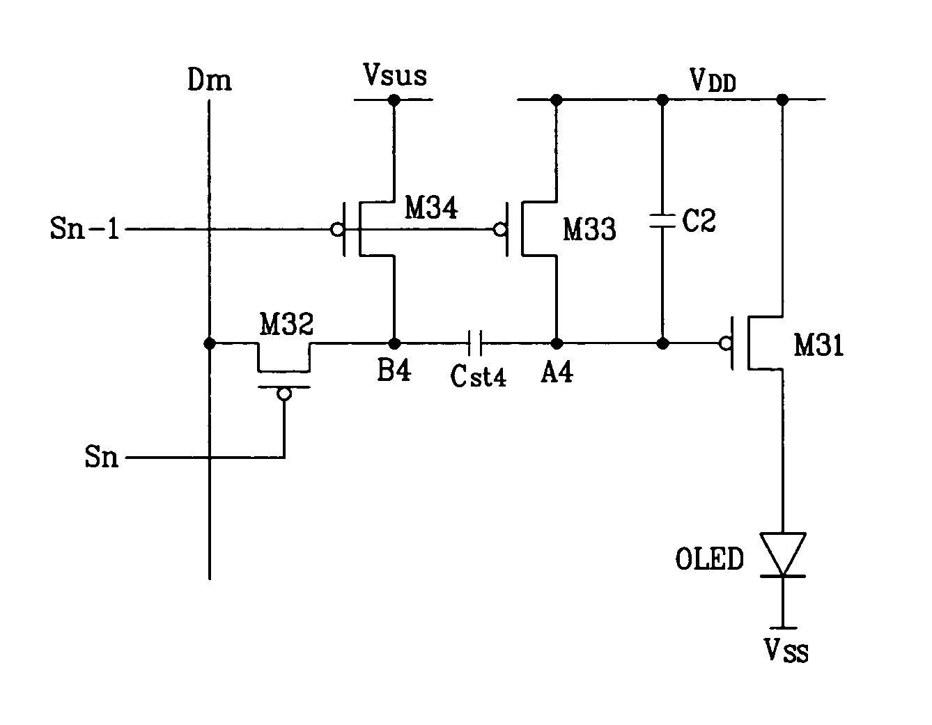
[0045] The organic EL display panel 100 includes a plurality of data lines D1 through Dm, each extending in a column direction, a plurality of scan lines S1 through Sn, each extending in a row direction, and a plurality of pixel circuits 10. The data lines D1 through Dm transmit data voltages that correspond to...


PUM


Abstract

A light emitting display including data lines for transmitting data voltages, scan lines for selecting select signals, and pixel circuits. The pixel circuit is coupled to a data line and a scan line. The pixel circuit includes a transistor including first, second, and third electrodes, wherein the third electrode outputs a current corresponding to a voltage between the first and second electrodes. A light emitting element coupled to the third electrode emits light corresponding to the current outputted by the third electrode. A first switch transmits a data voltage in response to a select signal from the scan line. A voltage compensator receives the data voltage transmitted by the first switch and a second power supply voltage and applies a compensated data voltage based on the data voltage, a first power supply voltage and the second power supply voltage to the first electrode of the transistor.

Description

CROSS REFERENCE TO RELATED APPLICATION [0001] This application claims priority to and the benefit of Korean Patent Application No. 2003-85067 filed on Nov. 27, 2003 in the Korean Intellectual Property Office, the entire content of which is incorporated herein by reference. BACKGROUND OF THE INVENTION [0002] (a) Field of the Invention [0003] The present invention relates to a light emitting display and a driving method thereof. More specifically, the present invention relates to an organic EL (electroluminescent) display. [0004] (b) Description of the Related Art [0005] In general, an organic EL display electrically excites a phosphorous organic compound to emit light, and it voltage- or current-drives N×M organic emitting cells to display images. As shown in FIG. 1, the organic emitting cell includes an anode (ITO), an organic thin film, and a cathode layer (metal). The organic thin film has a multi-layer structure including an EML (emitting layer), an ETL (electron transport layer)...

Claims


Application Information

Patent Timeline
Patent Type & Authority Applications(United States)
IPC IPC(8): G09F9/30H01L51/50G09G3/20G09G3/30H01L27/32H05B44/00
CPCG09G3/3233G09G2300/043G09G2300/0819G09G2300/0842G09G2320/043G09G2310/0262G09G2320/02G09G2320/0223G09G2310/0251G09G3/30
Inventor KIM, YANG-WANOH, CHOON-YULKIM, KYOUNG-DO
Owner SAMSUNG DISPLAY CO LTD
Why Eureka
Try Eureka