In-plane switching mode liquid crystal display device and method of fabricating the same

a liquid crystal display and switching mode technology, applied in non-linear optics, instruments, optics, etc., can solve the problems of limiting the fabrication of large-sized lcd devices, deteriorating image quality of ips mode lcd devices, so as to prevent color shift, prevent color shift, and uniform image quality

a liquid crystal display and switching mode technology, applied in non-linear optics, instruments, optics, etc., can solve the problems of limiting the fabrication of large-sized lcd devices, deteriorating image quality of ips mode lcd devices, so as to prevent color shift, prevent color shift, and uniform image quality

US20050140896A1Active Publication Date: 2005-06-30LG DISPLAY CO LTD

Image

  • In-plane switching mode liquid crystal display device and method of fabricating the same
  • In-plane switching mode liquid crystal display device and method of fabricating the same
  • In-plane switching mode liquid crystal display device and method of fabricating the same

Examples


Embodiment Construction

[0036] Reference will now be made in detail to the preferred embodiments of the present invention, examples of which are illustrated in the accompanying drawings.

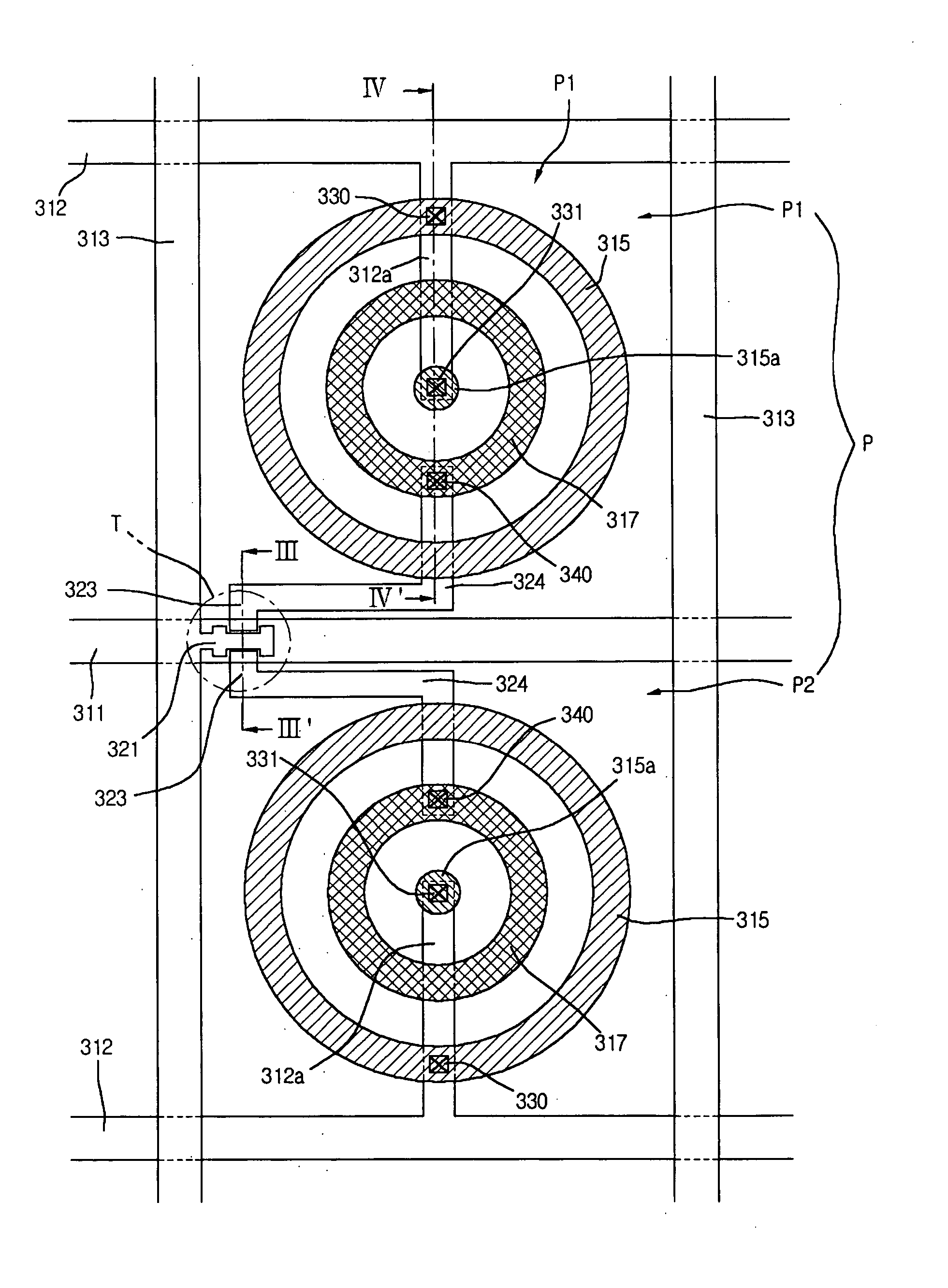
[0037]FIG. 3 is a partial plan view of an exemplary lower substrate of an IPS mode LCD device according to the present invention. In FIG. 3, a unit pixel P of an IPS mode LCD device may be bordered by a pair of adjacent data lines 313 extending along a first direction and may include a gate line 311 extending along a second direction perpendicular to the first direction, wherein the data lines 313 may cross the gate lines 311. In addition, common electrode lines 312 may be provided to be spaced apart by a distance from the gate line 311 along the first direction. Accordingly, the unit pixel P may include a pair of first and second pixel regions P1 and P2.

[0038] The gate line 311 may extend through a middle portion of the unit pixel P, wherein the first pixel region P1 may be formed between the gate line 311 and a first li...


PUM


Abstract

A liquid crystal display device includes first and second common electrode lines on a substrate extending along a first direction, a pair of adjacent data lines extending along a second direction perpendicular to the first direction to cross the first and second common electrode lines to define a unit pixel region, a gate line extending between the first and second common electrode lines along the first direction and crossing the pair of adjacent data lines, the first and second common electrode lines spaced apart from the gate line by a first distance along the second direction defining a first pixel region and a second pixel region of the unit pixel region, and a thin film transistor formed at the crossing of the gate line and one of the pair of adjacent data lines, the thin film transistor including a pair of drain electrodes, a source electrode, and a portion of the gate line, wherein each of the first and second pixel regions includes a circular pixel electrode and first and second circular common electrodes.

Description

[0001] The present invention claims the benefit of Korean Patent Application No. 98614 / 2003 filed in Korea on Dec. 29, 2003, which is hereby incorporated by reference. BACKGROUND OF THE INVENTION [0002] 1. Field of the Invention [0003] The present invention relates to a liquid crystal display (LCD) device and a method of fabricating an LCD device, and more particularly, to an In-Plane Switching (IPS) mode LCD device and a method of fabricating an IPS mode LCD device. [0004] 2. Description of the Related Art [0005] In general, an LCD device is formed by attaching an upper substrate and a lower substrate and injecting a liquid crystal into a space between the upper substrate and the lower substrate. In addition, a polarizer and a retardation film are attached on outer surfaces of the upper substrate and the lower substrate. Accordingly, by selectively arranging functional elements of the LCD device, an advancing direction or refractive index of light is changed, thereby forming an LCD...

Claims


Application Information

Patent Timeline
30 Jun 2005
Publication
US20050140896A1
IPC
G02F1/1343
CPC
G02F2201/122; G02F1/134363; G02F1/1343
Inventors
CHAE, GEE SUNG; LEE, YUN BOK