1 x N fanout waveguide photodetector

a waveguide and photodetector technology, applied in the field of photodetectors, can solve the problems of low carrier collection efficiency, low absorption coefficient, and detection of speeds of 2 ghz or less

Inactive Publication Date: 2005-07-07
INTEL CORP
View PDF22 Cites 32 Cited by
  • Summary
  • Abstract
  • Description
  • Claims
  • Application Information

AI Technical Summary

Problems solved by technology

To date, it has been a challenge to make a Si-based semiconductor PIN photodetector with a bandwidth of 10 GHz or greater.
Conventional discrete PIN Si detectors operate at speeds of 2 GHz or less because of their relatively low absorption coefficient and low carrier collection efficiency.
It is well known that excess optical power density in PIN photodetectors causes detector speed degradation.
As a result, the detector may not be able to operate at high photocurrent where high-speed operation may require a high current.
However, the light distribution in the expanded waveguide region (i.e., the waveguide plus the intrinsic region) is not uniform so that the detector electrodes need to be made relative large to ensure adequate detection of the photon-generated carriers.
Unfortunately, the relatively large electrode area results in a relatively high detector capacitance, which reduces detector speed.
Further, the non-uniform distribution of light in the expanded waveguide region can result in high optical fields, which generate local excess photon-generated carriers.
This reduces the detector speed when the excess carriers have to diffuse out of the local excess carrier area to be collected by the electrodes.
This thickness, however, limits the detector speed.
In the latter design, photon-generated carriers also have to travel to the interdigitated electrodes across the detector, so that the detector thickness also limits the detector speed.

Method used


Image

  • 1 x N fanout waveguide photodetector
  • 1 x N fanout waveguide photodetector
  • 1 x N fanout waveguide photodetector

Examples


Embodiment Construction

[0023] In the following detailed description of the embodiments of the invention, reference is made to the accompanying drawings that form a part hereof, and in which is shown by way of illustration specific embodiments in which the invention may be practiced. These embodiments are described in sufficient detail to enable those skilled in the art to practice the invention, and it is to be understood that other embodiments may be utilized and that changes may be made without departing from the scope of the present invention. The following detailed description is, therefore, not to be taken in a limiting sense, and the scope of the present invention is defined only by the appended claims.

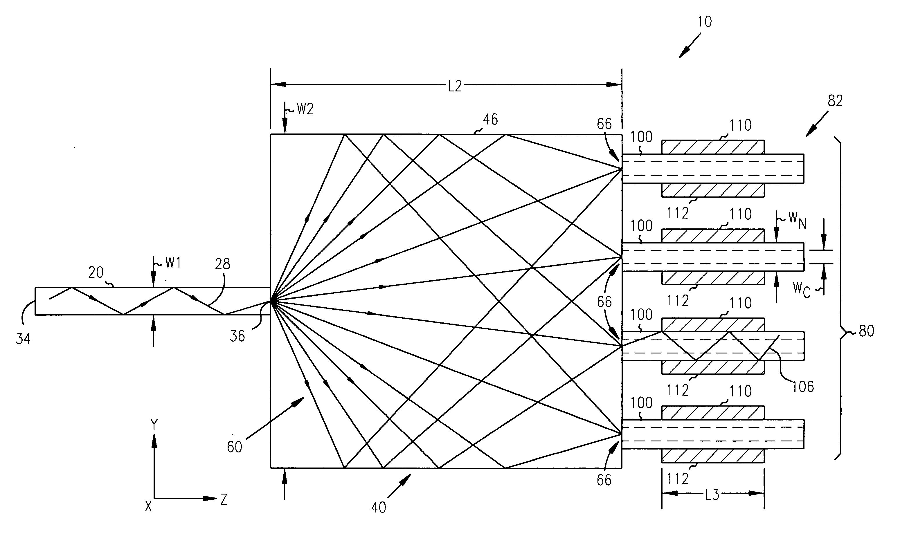
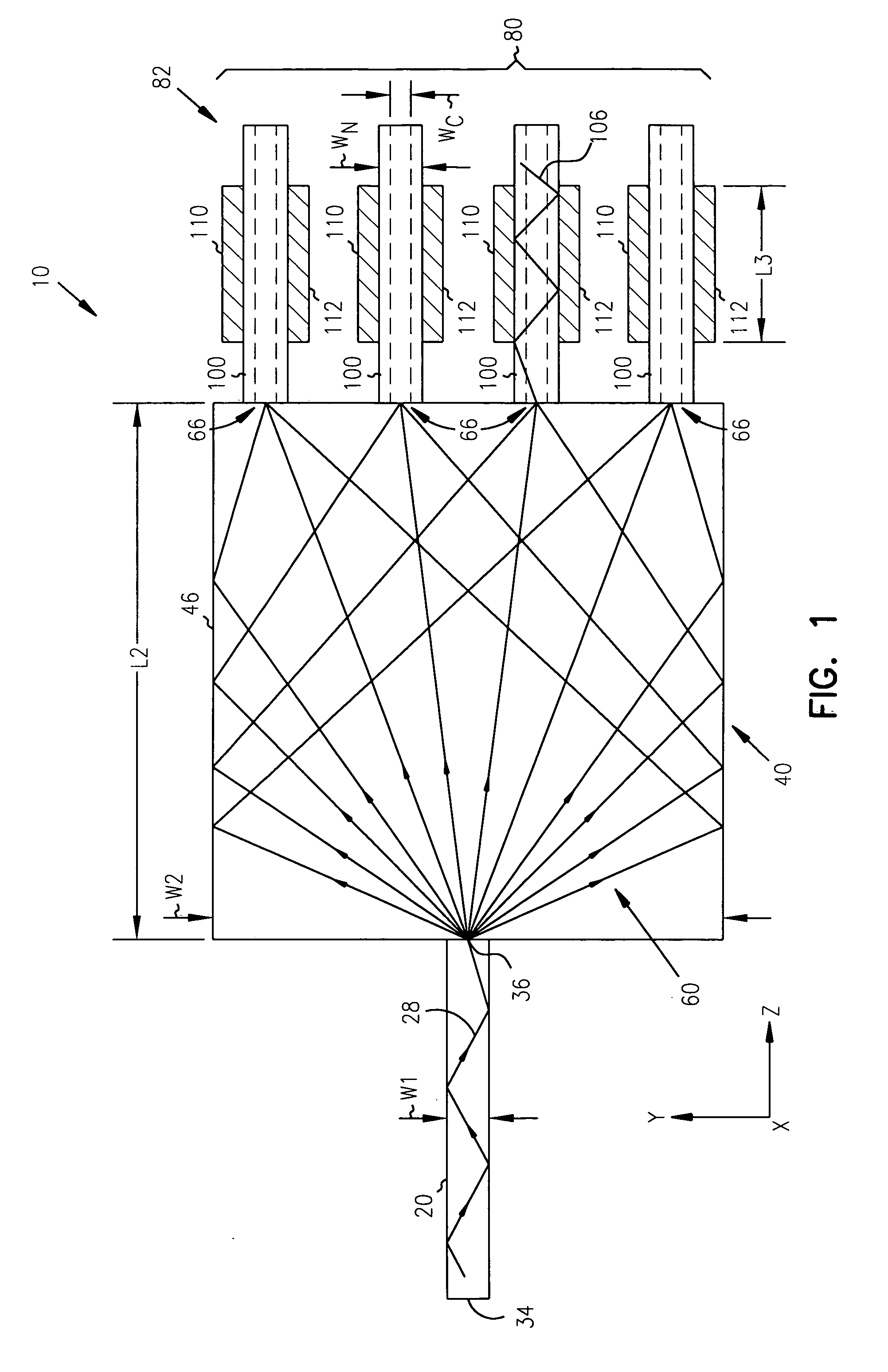
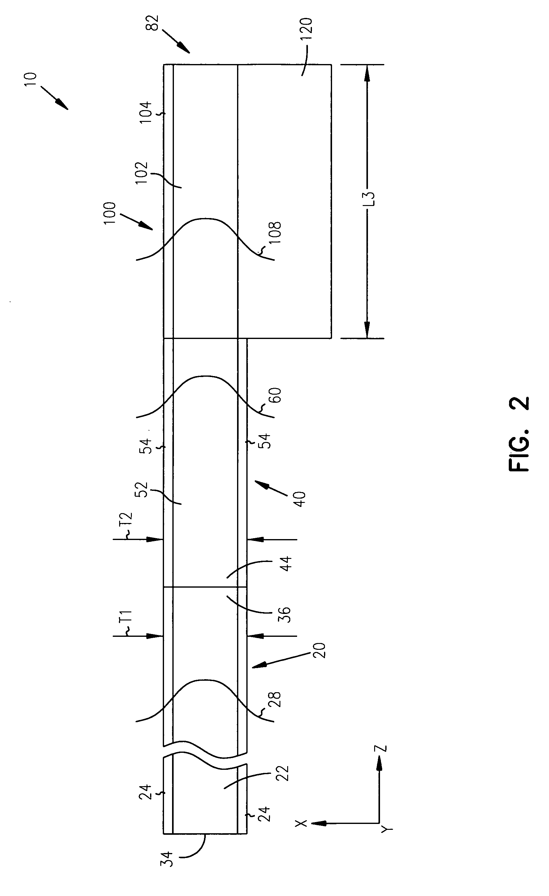
[0024] With reference to FIGS. 1 and 2, there is shown an integrated waveguide-based photodetector system 10 comprising an input waveguide 20 having a core 22 and a cladding 24. In an example embodiment, the waveguide is designed to support a single waveguide mode 28, as illustrated schematically in ...


PUM


Abstract

A 1×N fanout waveguide detector is disclosed. The detector includes a multiple-mode interference (MMI) cavity with input and output ends. A single-mode waveguide is optically coupled to the input end of the MMI cavity so that the optical power in the guided mode is distributed over N modes. The MMI cavity forms N interference nodes at or near its output end. N waveguide detectors are optically coupled to the output end at or near the N interference nodes. The waveguide detectors each have a waveguide that is evanescently coupled to an intrinsic region of a PIN detector. The width of the detector waveguide core, which can be sub-micron, defines the carrier collection distance between the electrodes of the PIN detector. Further, the length of the detector waveguide can be selected to maximize optical absorption to provide optimum quantum efficiency. The waveguide detectors are connected in parallel to provide a high-output photocurrent.

Description

RELATED APPLICATION(S) [0001] This application is a Divisional of U.S. application Ser. No. 10 / 008,922 filed Dec. 7, 2001 which is incorporated herein by reference.FIELD OF THE INVENTION [0002] The present invention pertains to photodetectors, and in particular to waveguide-based high-speed photodetectors. BACKGROUND OF THE INVENTION [0003] There are many lightwave applications, such as optical telecommunications and chip interconnects, that involve transmitting optical signals and converting them to electrical signals at high data rates. The systems for performing such transmission and conversion usually require a photodetector compatible with the speed and bandwidth of the optical signal. The typical photodetectors are PIN (p-type / intrinsic semiconductor material / n-type) semiconductor detectors. [0004] To date, it has been a challenge to make a Si-based semiconductor PIN photodetector with a bandwidth of 10 GHz or greater. Conventional discrete PIN Si detectors operate at speeds o...

Claims


Application Information

Patent Timeline
Patent Type & Authority Applications(United States)
IPC IPC(8): G02B6/12G02B6/28G02B6/42G02B6/43
CPCG02B6/12004G02B6/2813G02B2006/1215G02B6/43G02B2006/12123G02B6/42
Inventor ZHENG, JUN F.
Owner INTEL CORP
Why Eureka
Try Eureka