Nitride semiconductor light emitting element

a light-emitting element and nitride technology, applied in semiconductor lasers, lasers, solid-state devices, etc., can solve the problems of inability to complete lattice matching, and numerous crystal defects referred to as threading dislocations, etc., to achieve good film quality, reduce reactive current and non-radiative recombination centers, and improve internal quantum efficiency

Inactive Publication Date: 2007-05-31
ROHM CO LTD
View PDF2 Cites 85 Cited by
  • Summary
  • Abstract
  • Description
  • Claims
  • Application Information

AI Technical Summary

Benefits of technology

[0007] In order to overcome the problems described above, preferred embodiments of the present invention provide a nitride semiconductor light-emitting element which suppresses and minimizes reactive currents and non-radiative recombination centers by pr

Problems solved by technology

When a sapphire substrate is used as the substrate, lattice mismatching with the nitride semiconductor layer laminated thereon reaches approximately 14%, so that complete lattice matching cannot be accomplished.
Furthermore, even if an SiC substrate is used, there is a high degree of lattice mismatching, so that complete lattice matching cannot be accomplished.
Accordingly, an extremely large number of crystal defects are produced in the nitride semiconductor layer that is caused to grow on the substrate, and the crystal defects also extend in the vertical direction through the nitride semiconductor layer that is laminated thereon, so that numerous crystal defects referred to as threading dislocations are present.
Therefore, there is a problem in that the emission efficiency (internal quantu

Method used


Image

  • Nitride semiconductor light emitting element
  • Nitride semiconductor light emitting element
  • Nitride semiconductor light emitting element

Examples


Embodiment Construction

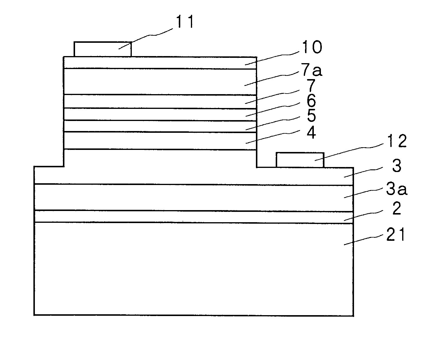
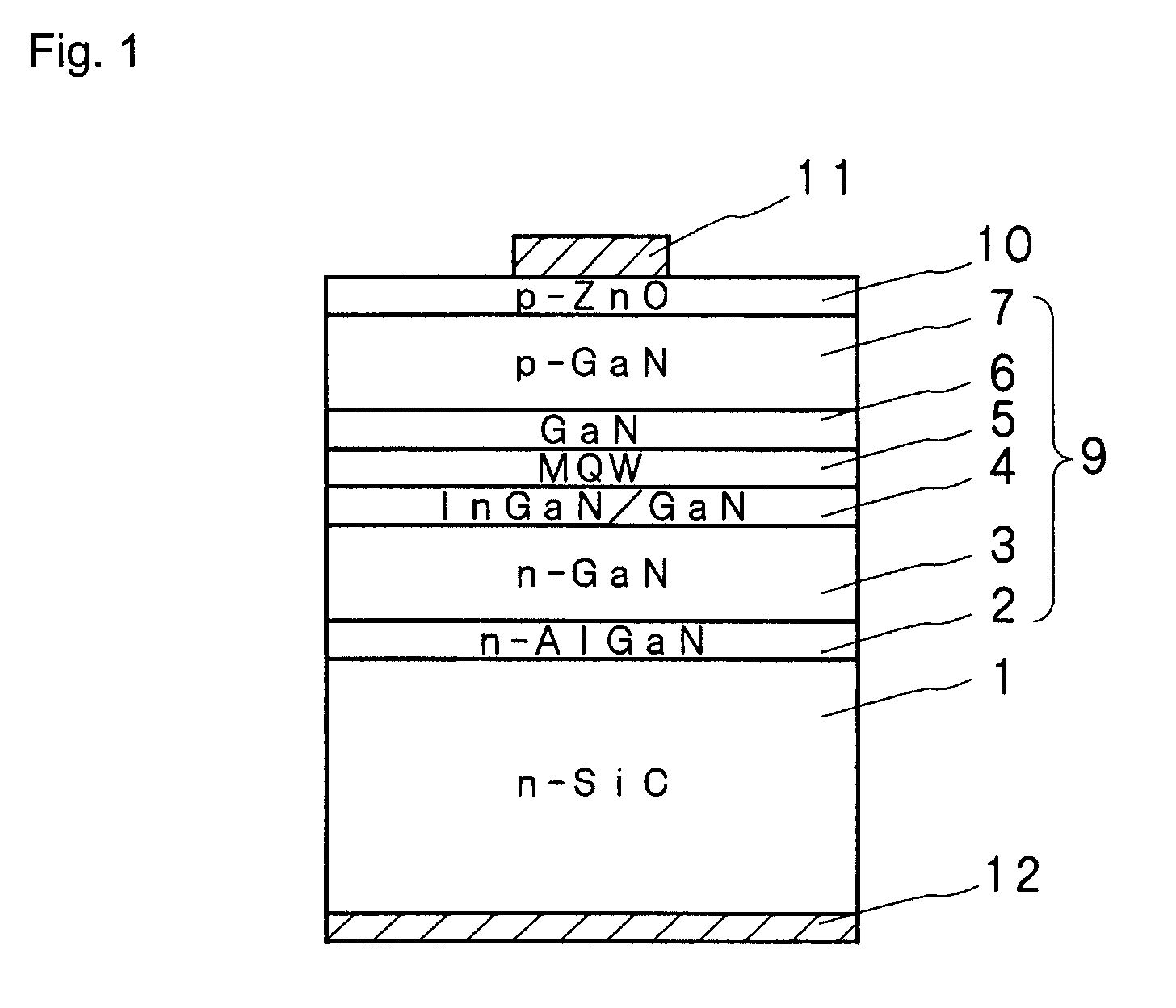
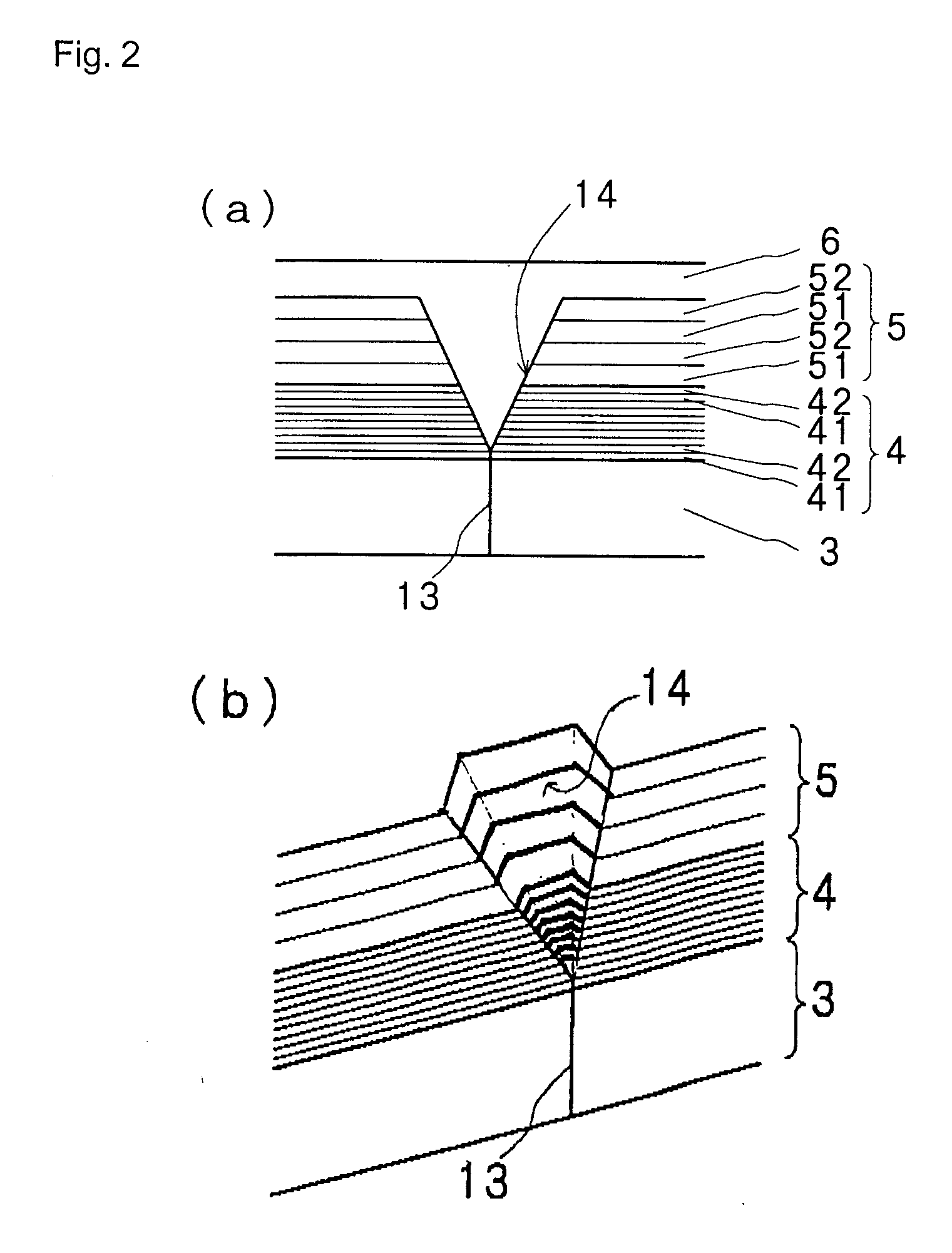
[0022] Nitride semiconductor light-emitting elements according to various preferred embodiments of the present invention will be described with reference to the figures. A sectional explanatory diagram of one preferred embodiment of the present invention is shown in FIG. 1. The nitride semiconductor light-emitting element according to the present preferred embodiment of the present invention preferably includes, on a substrate 1, a nitride semiconductor lamination portion including at least an active layer 5 for forming a light-emitting portion, and a pit formation layer 4 disposed on the side of the substrate 1 of the active layer 5 in a superlattice structure of a nitride semiconductor and arranged to generate pits in the end portions of threading dislocations generated in the nitride semiconductor layer on the side of the substrate 1.

[0023] In order to suppress a leakage current which occurs as a result of threading dislocations that tend to be generated in the nitride semicondu...


PUM


Abstract

A nitride semiconductor light-emitting element suppresses leakage currents and non-radiative recombination centers by providing, as an underlying layer of the active layer, a pit formation layer that reliably generates pits, while maintaining a good film quality, so that the internal quantum efficiency is improved, and the light-emitting characteristics are also improved. A nitride semiconductor lamination portion including at least an active layer for forming a light-emitting portion is present on a substrate, and a pit formation layer is formed as a superlattice layer of nitride semiconductor on the side of the substrate of the active layer. The pit formation layer generates pits in the end portions of threading dislocations that are generated in the nitride semiconductor layer on the side of the substrate.

Description

BACKGROUND OF THE INVENTION [0001] 1. Field of the Invention [0002] The present invention relates to a light-emitting element using a nitride semiconductor, and more particularly, the present invention relates to a nitride semiconductor light-emitting element which prevents threading dislocations from extending into an active layer and increasing leakage currents by reliably generating pits underneath the active layer, thus improving brightness. [0003] 2. Description of the Related Art [0004] Conventional light-emitting elements using a nitride semiconductor are formed by growing a nitride semiconductor lamination portion that contains a buffer layer and a light-emitting layer formation portion on, for example, a sapphire substrate, etching a portion of this semiconductor lamination portion to expose a conductor formation layer on the lower side of the semiconductor lamination portion, and respectively providing a lower electrode on the exposed surface of the lower-side conductor fo...

Claims


Application Information

Patent Timeline
IPC IPC(8): H01L33/00H01L21/76H01L33/06H01L33/32
CPCB82Y20/00H01L33/007H01L33/02H01S5/021H01S5/0421H01S5/3216H01S5/34333H01S2301/173
Inventor SONOBE, MASAYUKIITO, NORIKAZU
Owner ROHM CO LTD
Why Eureka
Try Eureka