Gallium nitride-on-silicon interface using multiple aluminum compound buffer layers

a technology of gallium nitride and silicon, applied in the field of integrated circuit (ic) fabrication, can solve the problems of limiting the use of sapphire in high power and high density device applications, affecting the thermal conductivity of sapphire, and affecting the performance of the device, etc., and achieves the effect of high power and high density devi

Inactive Publication Date: 2009-10-06
SHARP KK
View PDF12 Cites 94 Cited by
  • Summary
  • Abstract
  • Description
  • Claims
  • Application Information

AI Technical Summary

Benefits of technology

[0015]As noted above, the current best large-area GaN films are grown on sapphire substrates. But, state-of-the-art sapphire substrate size is relatively small and expensive. Further, the thermal conductivity of sapphire is low [0.349 (W / cm-° C.)], which limits their use in high power and high density device applications. The high cost of large sapphire substrates makes GaN-on-silicon substrates the best alternative. Si substrates have a higher thermal conductivity [1.49 (W / cm-° C.)], which is four times higher than sapphire.
[0016]The lattice constants of GaN, Si, and sapphire are about 0.32 nm, 0.38 nm, and 0.48 nm, respectively. Thus, the lattice mismatch between GaN and sapphire is more severe than that between GaN and silicon. However, the thermal expansion coefficients for GaN, Si, and sapphire are about 5.6×10⁻⁶ / ° K., 3.7×10⁻⁶ / ° K., and 7.4×10⁻⁶ / ° K., respectively. Thus, the thermal expansion mismatch between GaN and Si is more severe than that between GaN and sapphire. To avoid the lattice mismatch and thermal mismatch between GaN and Si, a nanoscale lateral epitaxial overgrowth process with aluminum compound buffer layers may be used to improve the GaN film quality. In addition, a nanoheteroepitaxy lateral overgrowth technology may be combined with the aluminum compound buffer layers to make high quality thick GaN films on Si substrates.

Problems solved by technology

But, state-of-the-art sapphire substrate size is relatively small and expensive.
)], which limits their use in high power and high density device applications.
Thus, the lattice mismatch between GaN and sapphire is more severe than that between GaN and silicon.
Thus, the thermal expansion mismatch between GaN and Si is more severe than that between GaN and sapphire.

Method used


Image

  • Gallium nitride-on-silicon interface using multiple aluminum compound buffer layers
  • Gallium nitride-on-silicon interface using multiple aluminum compound buffer layers
  • Gallium nitride-on-silicon interface using multiple aluminum compound buffer layers

Examples


Embodiment Construction

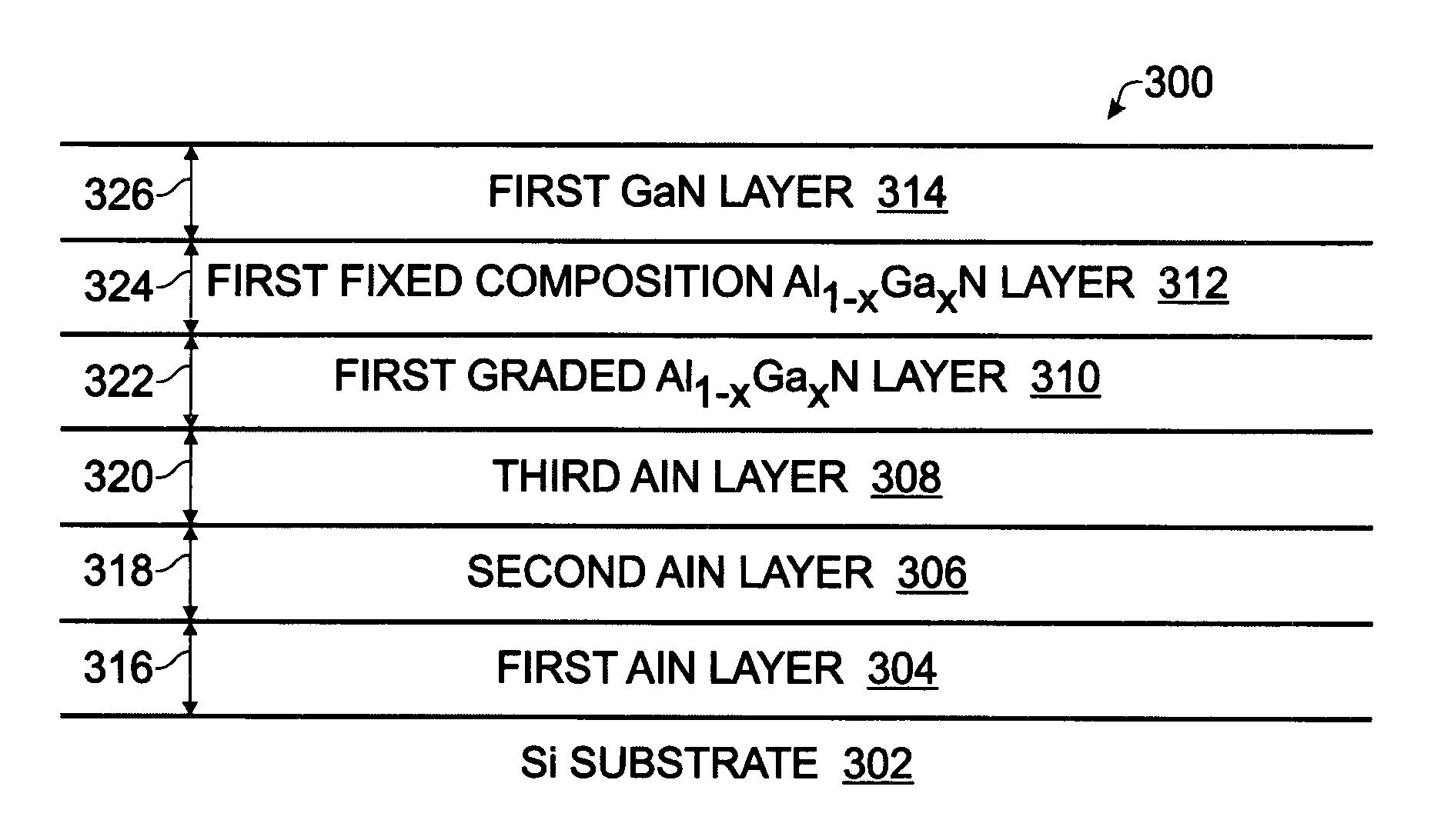
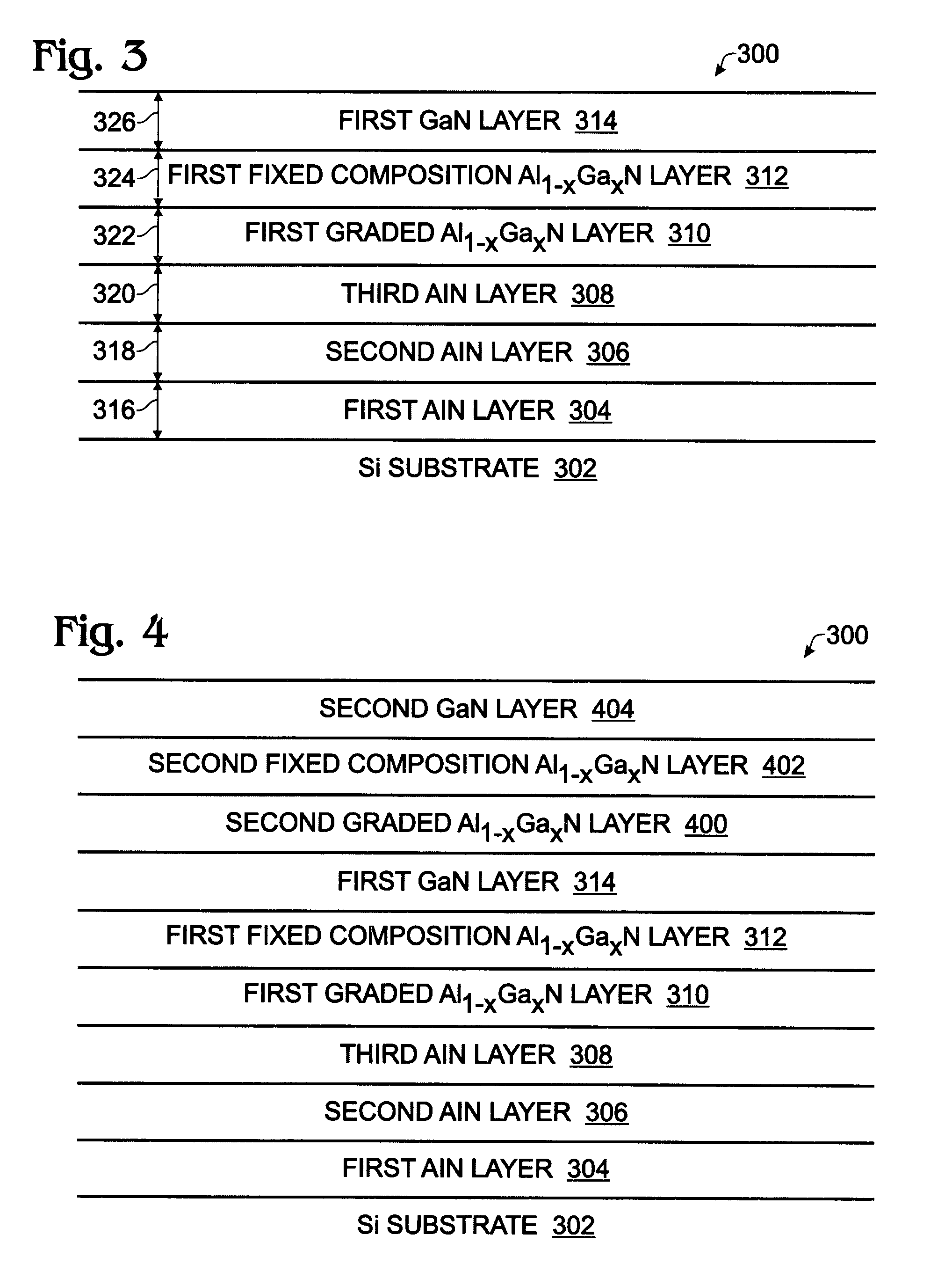
[0029]FIG. 3 is a partial cross-sectional view of a silicon (Si)-to-gallium nitride (GaN) thermal expansion interface with multiple aluminum compound buffer layers. The interface 300 comprises a (111) Si substrate 302 and a first layer of AlN 304 overlying the substrate having a first density. A second layer of AlN 306 overlies the first layer of AlN having a second density, less than the first density. A third layer of AlN 308 overlies the second layer of AlN 306, having the first density. That is, third AlN layer 308 is denser than second layer 306. However, the density of the first layer 304 need not be identical to the density of the third layer 308. A first grading Al1-XGaXN layer 310 overlies the third layer of AlN 308, where 01-XGaXN layer 312 overlies the first grading Al1-XGaXN layer 310, where 0314 overlies the first fixed composition Al1-XGaXN layer 312.

[0030]In one aspect, the first and second AlN layers 304 and 306 each have a thickness 316 and 318, respectively, in the...


PUM

PropertyMeasurementUnit
temperatureaaaaaaaaaa
thicknessaaaaaaaaaa

Abstract

A thermal expansion interface between silicon (Si) and gallium nitride (GaN) films using multiple buffer layers of aluminum compounds has been provided, along with an associated fabrication method. The method provides a (111) Si substrate and deposits a first layer of AlN overlying the substrate by heating the substrate to a relatively high temperature of 1000 to 1200° C. A second layer of AlN is deposited overlying the first layer of AlN at a lower temperature of 500 to 800° C. A third layer of AlN is deposited overlying the second layer of AlN by heating the substrate to the higher temperature range. Then, a grading Al1-XGaXN layer is formed overlying the third layer of AlN, where 0<X<1, followed by a fixed composition Al1-XGaXN layer overlying the first grading Al1-XGaXN layer. An epitaxial GaN layer can then be grown overlying the fixed composition Al1-XGaXN layer.

Description

BACKGROUND OF THE INVENTION[0001]1. Field of the Invention[0002]This invention generally relates to integrated circuit (IC) fabrication and, more particularly to a gallium nitride-on-silicon interface that uses multiple buffer layers of aluminum compounds, and an associated fabrication process.[0003]2. Description of the Related Art[0004]Gallium nitride (GaN) is a Group III / Group V compound semiconductor material with wide bandgap (3.4 eV), which has optoelectronic, as well as other applications. Like other Group III nitrides, GaN has a low sensitivity to ionizing radiation, and so, is useful in solar cells. GaN is also useful in the fabrication of blue light-emitting diodes (LEDs) and lasers. Unlike previous indirect bandgap devices (e.g., silicon carbide), GaN LEDs are bright enough for daylight applications. GaN devices also have application in high power and high frequency devices, such as power amplifiers.[0005]GaN LEDs and GaN-based devices are conventionally fabricated using ...

Claims


Application Information

Patent Timeline
Patent Type & Authority Patents(United States)
IPC IPC(8): H01L21/00
CPCH01L21/02381H01L21/02458H01L21/02505H01L21/0251H01L29/205H01L21/0262H01L29/155H01L29/2003H01L21/0254H01L21/02647
Inventor LI, TINGKAITWEET, DOUGLAS J.MAA, JER-SHENHSU, SHENG TENG
Owner SHARP KK
Why Eureka
Try Eureka