Semiconductor module

a technology of semiconductor modules and modules, applied in the direction of semiconductor devices, semiconductor/solid-state device details, diodes, etc., can solve the problems of large calorific value and achieve the effects of high accuracy, excellent moisture resistance and voltage endurance characteristics, and convenient laminated

Inactive Publication Date: 2014-11-20
TOYOTA JIDOSHA KK
View PDF10 Cites 16 Cited by
  • Summary
  • Abstract
  • Description
  • Claims
  • Application Information

AI Technical Summary

Benefits of technology

[0011]The device package is formed by molding the electronic component by resin, and it is possible to mold the electronic component with high accuracy in terms of size in its thickness direction. On that account, the molding is convenient to be laminated with the semiconductor package by use of the cooling plates. Further, a resin mold is excellent in moisture resistance and voltage endurance characteristics. Particularly, the resin mold is excellent in voltage endurance characteristics, so that the resin mold is convenient to be placed close to the semiconductor package. The semiconductor element and the electronic component through which heavy-current flows are connected via conductive members called bus bars. The bus bar is a metal long-plate-like member having a high voltage endurance. The device package excellent in voltage endurance characteristics is also convenient to be placed close to such bus bars.
[0012]A load is added to the laminated body of the cooling plates, the semiconductor packages, and the device packages from both sides in a laminating direction, so that adherence between the cooling plates and the semiconductor packages (or the device packages) is increased. By increasing the adherence, thermal conductivity between the semiconductor package (or the device package) and the cooling plate is increased. A thickness of the semiconductor package is generally equal to a thickness of the device package, and the cooling plate may have a structure in which its thickness is changed according to the load in the laminating direction. Here, an example of the “structure in which the thickness is changed” is such that part of a side wall of the cooling plate or the cooling tube has an accordion structure or a bellows structure, and a thickness of the accordion structure or the bellows structure shrinks according to the load. As described earlier, the load is added to the semiconductor module from both sides in the laminating direction. Here, since the thickness of the semiconductor package is equal to the thickness of the device package, the thicknesses between the cooling plates are equally narrowed according to the load, thereby making it possible to prevent breakage of the cooling plates.
[0013]A typical example of the electronic component housed in the device package is a capacitor. The capacitor may be a flat wound capacitor or may be a laminated capacitor. The flat wound capacitor is cheaper than the laminated capacitor. The laminated capacitor can be formed easily to be thin in comparison with the wound capacitor.
[0014]A resin mold of the device package may be molded by potting or spraying. Differently from transfer molding commonly used for a semiconductor element, the potting or the spraying does not need to increase a temperature and a pressure of the electronic component, so that it is suitable for molding of an electronic component that does not have a high heat resistance.
[0015]The semiconductor package and the device package may be disposed adjacent to each other in one layer between two cooling plates, or may be disposed in different layers. In the first case, it is possible to shorten a length of the semiconductor module in the laminating direction. In the latter case, it is possible to reduce a width of the semiconductor module. Further, in an example of the latter case, at least one semiconductor package and at least one device package may be disposed to overlap with each other when viewed from the laminating direction. Alternatively, at least one semiconductor package and at least one device package may be disposed side by side in a lateral direction between two cooling plates adjacent to each other. In other words, at least one semiconductor package and at least one device package may be disposed side by side in a direction intersecting with the laminating direction.
[0016]It is preferable that the semiconductor element in the semiconductor package be electrically connected to the electronic component in the device package via linear bus bars. In other words, it is preferable that the semiconductor element in the semiconductor package be connected to the electronic component in the device package via the bus bars with a shortest distance. By connecting the semiconductor element to the electronic component via shortest bus bars, it is possible to reduce inductance of the bus bars. This makes it possible to reduce a surge current in switching of the semiconductor element. This leads to a decrease of switching loss of the semiconductor element.

Problems solved by technology

Since the current flowing between the source and the. drain of the power element is large, a capacitance of the smoothing capacitor becomes large, so that its calorific value also becomes large.

Method used


Image

  • Semiconductor module
  • Semiconductor module
  • Semiconductor module

Examples


Embodiment Construction

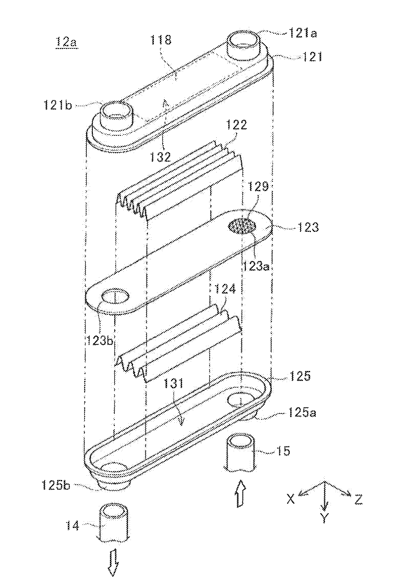
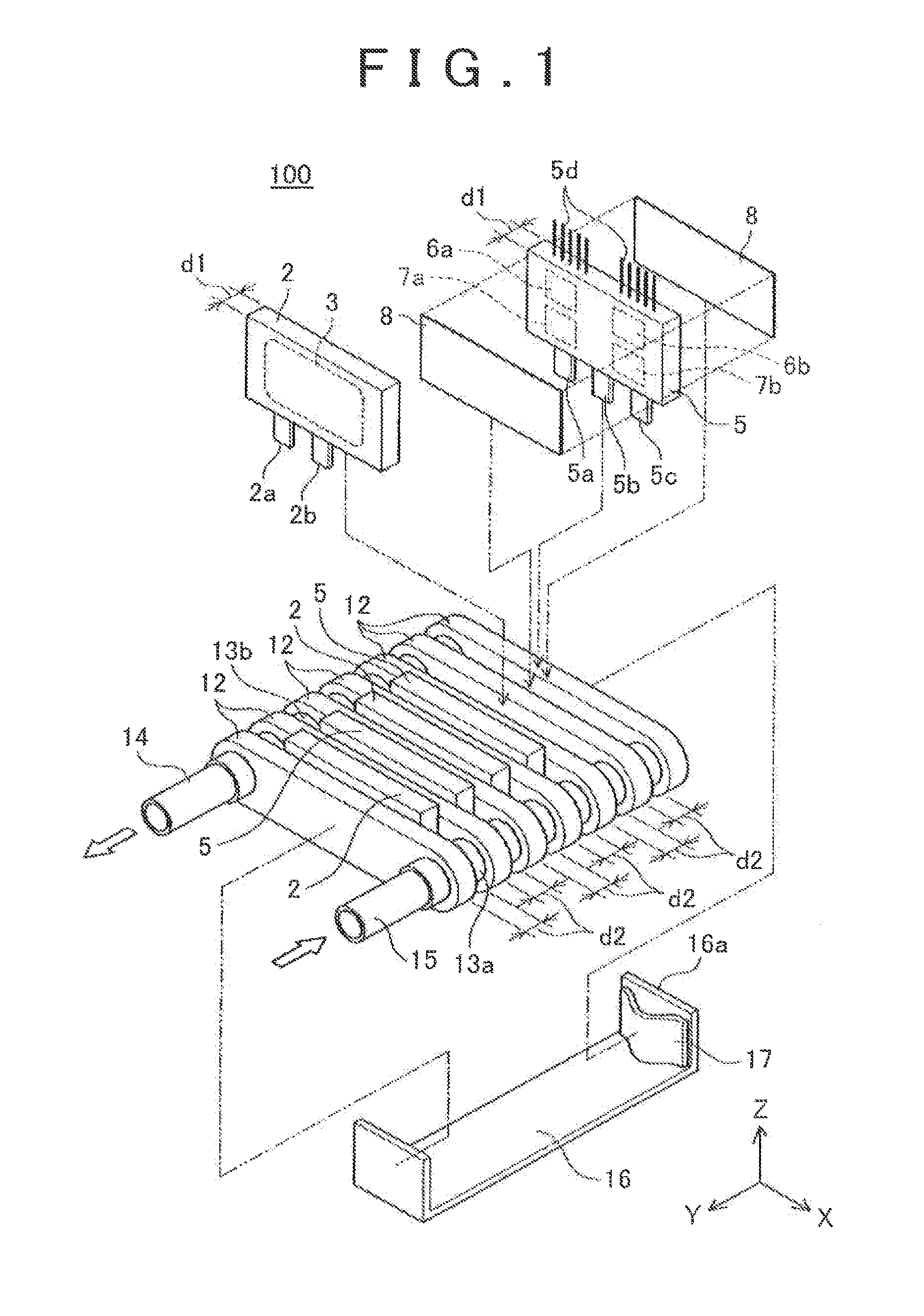
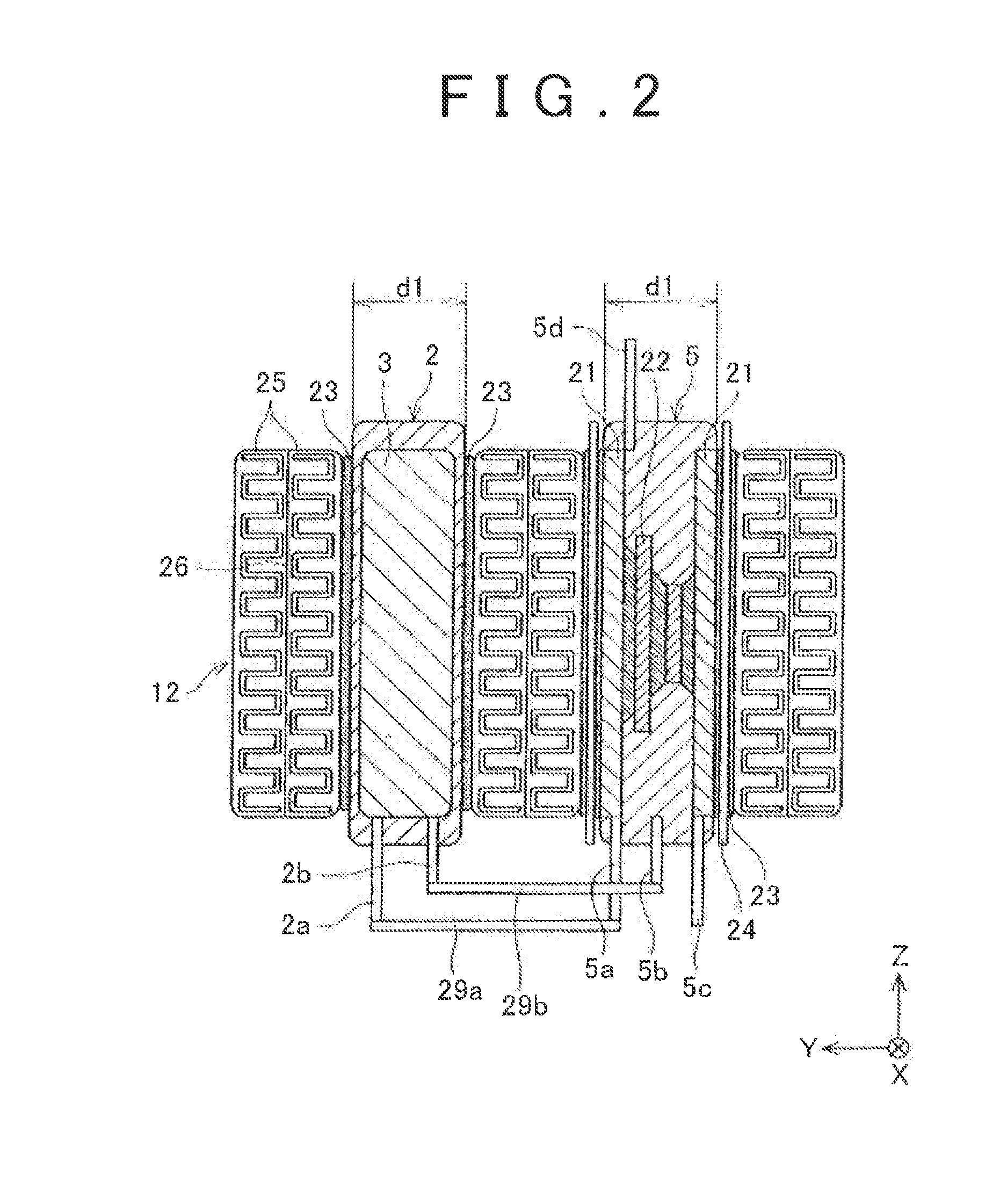
[0036]A semiconductor module according to an embodiment is described with reference to the drawings. FIG. 1 is a perspective view of a semiconductor module 100. Note that some components are illustrated separating from a main body in FIG. 1. The semiconductor module 100 is a module incorporated in a motor controller unit of an electric vehicle, and a transistor and a diode constituting a switching element of an inverter, and a smoothing capacitor are integrated therein. The semiconductor module 100 is mainly constituted by a plurality of cooling plates 12, a plurality of flat-plate semiconductor packages 5, and a plurality of device packages 2 each including a capacitor 3. Refrigerant flows inside the cooling plates 12, so that the refrigerant takes heat from the semiconductor packages 5 and the device packages 2 to cool off those packages.

[0037]The plurality of cooling plates 12 is disposed in parallel to each other, and the semiconductor package 5 or the device package 2 is sandwi...


PUM


Abstract

Provided is an improved cooler-integrated semiconductor module.
A semiconductor module (100) includes a plurality of cooling plates (12), and a plurality of flat-plate semiconductor packages (5) and flat-plate device packages (2). The semiconductor packages (5) each include a semiconductor element housed therein. The device packages (2) each include an electronic component housed therein, the electronic component being different in type from the semiconductor element housed in the semiconductor elements. The cooling plates (12) are laminated alternately with the semiconductor packages (5) or the device packages (2). Connecting tubes (13a, 13b) having refrigerant flowing therein are provided between the cooling plates (12) adjacent to each other.

Description

TECHNICAL FIELD[0001]The present invention relates to a semiconductor module in which a cooler is integrated with a plurality of flat-plate semiconductor packages each including a semiconductor element housed therein.BACKGROUND ART[0002]Semiconductor elements such as an IGBT and a reflux diode used in an inverter and a voltage converter have a large calorific value. Those elements may be called a power semiconductor element or simply a power element. The calorific value depends on a current magnitude to flow. Accordingly, the inverter for supplying an electric power to a motor for driving wheel assemblies (a drive motor for an electric vehicle including a hybrid vehicle), and the voltage converter are required to provide a large output, and use many power elements having a large calorific value. As well as the power elements, an electronic component having a large calorific value is used in the inverter and the voltage converter. A typical example of such an electronic component is ...

Claims


Application Information

Patent Timeline
Patent Type & Authority Applications(United States)
IPC IPC(8): H01L23/473H01L23/50H01L27/06H01L25/16H01L23/367
CPCH01L23/473H01L25/16H01L23/50H01L27/0629H01L23/3675H01L23/3107H01L23/4093H01L24/32H01L24/33H01L25/117H01L2224/32245H01L2224/33181H01L2924/13055H01L2924/19041H01L2924/19105H01L2924/00
Inventor HOTTA, KOJI
Owner TOYOTA JIDOSHA KK
Why Eureka
Try Eureka