Eureka AIR delivers breakthrough ideas for toughest innovation challenges, trusted by R&D personnel around the world.

Production method of metallized substrate

a production method and substrate technology, applied in the direction of conductive pattern formation, metal/alloy conductors, conductors, etc., can solve the problems of large amount of electric current, increased wiring resistance, difficult to form metal patterns with high dimensional precision, etc., to achieve favorable electric conductivity of metal layer 50, effectively inhibiting diffusion migration of titanium components, and good platability of metal layer 50

Active Publication Date: 2012-12-20
TOKUYAMA CORP
View PDF9 Cites 13 Cited by
  • Summary
  • Abstract
  • Description
  • Claims
  • Application Information

AI Technical Summary

Benefits of technology

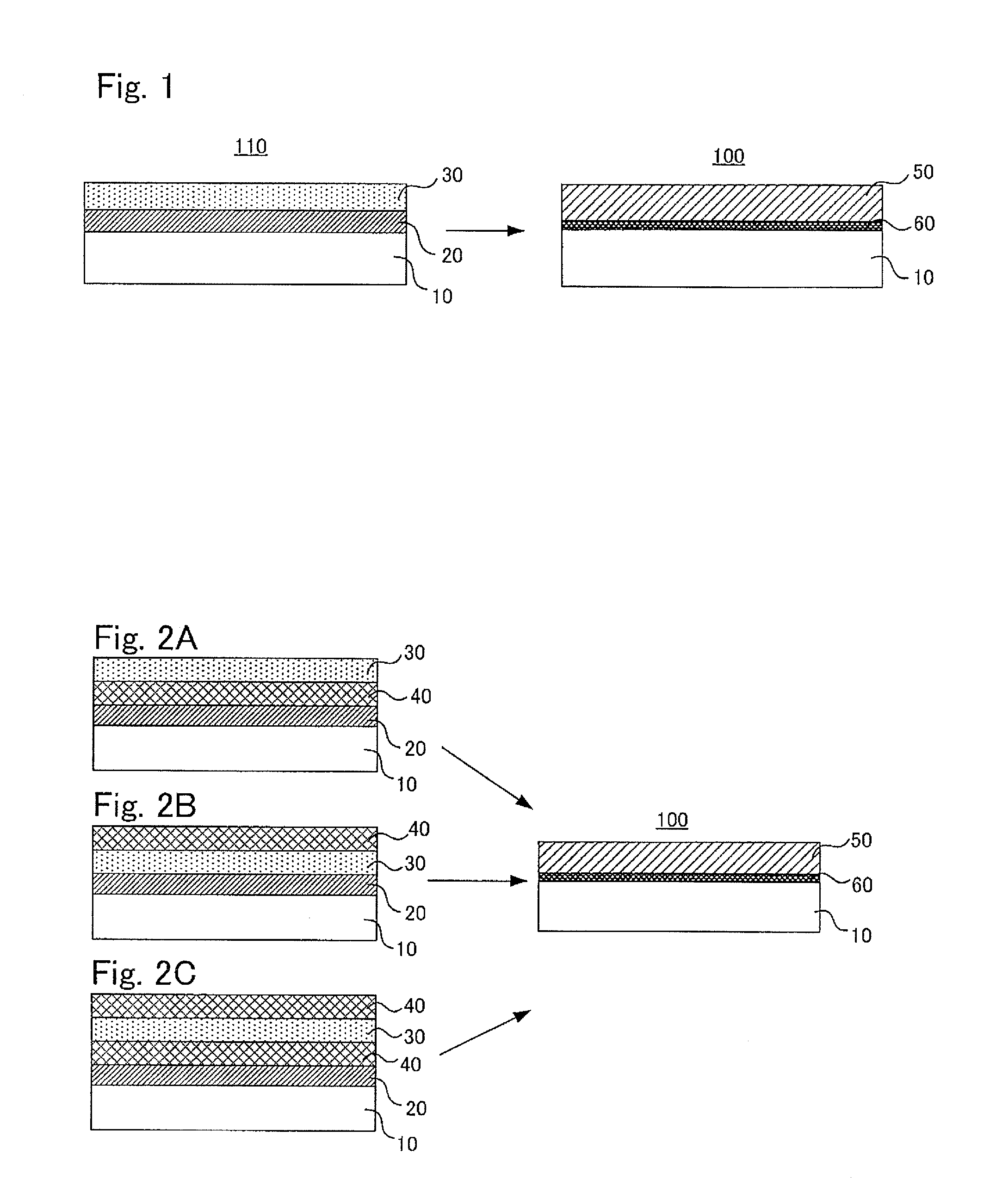
[0019]According to the production method of the first aspect of the present invention, the metal layer (50) is composed mainly of a copper component and a silver component, therefore enabling the electrical conductivity of the metal layer (50) to be favorable. Further, titanium hydride powder is contained only in the first paste layer which contacts the sintered nitride ceramic substrate (10), and the second paste layer not containing the titanium component is formed on the first paste layer, therefore causing reaction (titanium-nitride-forming reaction) between the titanium component and the nitride ceramic of the sintered substrate to occur preferentially at the time of firing, and effectively inhibiting diffusion migration of the titanium component toward the surface of the metal layer (50). As a result, the titanium nitride layer (60) is formed between the metal layer (50) and the sintered body (10); and therefore not only the adhesiveness but also the platability of the metal layer (50) can be favorable. Moreover, in the present invention, the paste containing, as the metal component, “copper-silver alloy powder” that can serve as a so-called brazing material is layered as the second paste layer (30). This alloy powder, which has a melting point lower than that of silver and copper, melts and liquefies during firing, and permeates into the first paste layer (20). This enables formation of the metal layer (50) with the reduced number and size of voids or with no voids at all; therefore, the adhesiveness of the metal layer (50) can be favorable, and as a result the thermal conductivity of the resultant metallized substrate (100) can be better. Furthermore, the surface smoothness of the metal layer (50) can be enhanced.
[0020]According to the production method of the second aspect of the present invention, by further forming the third paste layer (40), it is possible to reduce unevenness on the surface of the metal layer (50) attributed to the lower layer and to enhance the surface smoothness thereof.
[0021]The composition of the third aspect of the present invention has a thixotropic property; thereby when the composition is screen-printed under common printing conditions (squeegee printing pressure and squeegee speed), it exhibits favorable fluidity when passing through the mesh of a screen printing plate, whereas having an adequately increased viscosity after passing through the mesh. Therefore, printing problems like bubbles, clogging of the plate, and bleeding can be inhibited. As such, by using the composition of the third aspect of the present invention in the production methods of the first and second aspects of the present invention, to form the first paste layer in a predetermined shape by the screen printing method, the shape of the opening portions (non-masking parts) of the screen printing plate can be reproduced more accurately, thus enabling formation of the metal layer (50) with enhanced shape precision. At this time, the operability (printability) does not degrade terribly. The mesh marks may remain on the surface of the first paste layer in this case; however, since the firing is carried out after layering the second paste layer, the remaining mesh marks are smoothed out, and as a result the metal layer (50) with enhanced surface smoothness can be formed.
[0022]Accordingly, with the production methods of the first and second aspects of the present invention and the composition of the third aspect of the present invention, a metallized substrate with a highly precise and highly fine wiring pattern can be easily and effectively produced. Further, the metal layer of the metallized substrate can be used as a marker as it has favorable visibility.

Problems solved by technology

Conventionally, an alumina sintered body has been used as the material for the wiring substrate; however, because of the insufficient thermal conductivity of the alumina sintered body, the possibility of using an aluminum nitride sintered body, which has higher thermal conductivity, is being considered.
Especially in the uses where the heat radiating capability is required, a large amount of electric current is often needed.
On the other hand, in the thick-film method, high-melting-point metal such as tungsten and molybdenum is often used to form metal wiring; and in this case, there is a problem that wiring resistance is increased.
This co-firing method has characteristics that although it enables a solidly adhered metal layer to be formed, it is difficult to form a metal pattern with high dimensional precision due to the shrinkage of the ceramic following the sintering thereof.
However, it has been difficult heretofore, by the post-firing method, to attain high bonding strength (adhesion strength) of the metal layer on the nitride ceramics.
However, there has not yet been established industrially a technique of forming a metal layer on a sintered nitride ceramic substrate by using different metal pastes that can lower the wiring resistance more.

Method used


Image

  • Production method of metallized substrate
  • Production method of metallized substrate
  • Production method of metallized substrate

Examples


example 1

Preparation of a Paste Composition 1

[0111]A mortar was used to pre-mix 15 parts by mass of copper powder having an average particle size of 0.3 μm, 82 parts by mass of copper powder having an average particle size of 2 μm, and 3 parts by mass of titanium hydride powder having an average particle size of 5 with a vehicle in which polyalkyl methacrylate was dissolved in terpineol; and thereafter a three-roll mill was used to subject the mixture to a dispersion treatment, thereby preparing a paste composition 1.

[0112](Preparation of a Paste Composition 2)

[0113]A mortar was used to pre-mix Ag—Cu alloy powder (BAg-8; composition: 72 weight % of silver-28 weight % of copper) having an average particle size of 6μm, with a vehicle in which polyalkyl methacrylate was dissolved in terpineol; and thereafter a three-roll mill was used to subject the mixture to a dispersion treatment, thereby preparing a paste composition 2.

[0114](Production of a Metallized Substrate)

[0115]The above paste compos...

examples 2 to 3

[0117]A metallized substrate was produced in the same manner as in Example 1, except that the material composition of the paste was as shown in Table 1; and was analyzed and evaluated in the following manner. The results are shown in Tables 2 and 3.

example 4

Embodiment Shown in FIG. 2a

[0118](Preparation of Paste Compositions 1 and 2)

[0119]Paste compositions 1 and 2 were prepared in the same manner as in Example 1, except that the material compositions of the pastes were as shown in Table 1.

[0120](Preparation of a Paste Composition 3)

[0121]A mortar was used to pre-mix 20 parts by mass of copper powder having an average particle size of 0.3 μm and 80 parts by mass of copper powder having an average particle size of 2 μm, with a vehicle in which polyalkyl methacrylate was dissolved in terpineol; and thereafter a three-roll mill was used to subject the mixture to a dispersion treatment, thereby preparing a paste composition 3.

[0122](Production of a Metallized Substrate)

[0123]The above paste composition 1 prepared was printed, by screen printing, onto a sintered aluminum nitride substrate (trade name: SH-30, manufactured by Tokuyama Corporation) having a thickness of 0.64 mm; and then was dried at 100° C. for 10 minutes to form a first past...


PUM


Abstract

A production method for a metallized substrate to produce a metallized substrate which comprises: a sintered nitride ceramic substrate; a titanium nitride layer formed on the sintered substrate; and a metal layer containing copper, silver and titanium formed on the titanium nitride layer. The method comprises: a step of layering a first paste layer containing copper powder and titanium hydride powder on the sintered nitride ceramic substrate, to produce a first layered body; a step of layering a second paste layer containing silver-copper alloy powder on the first paste layer of the first layered body, to produce a second layered body; and a step of firing the second layered body, to thereby form the titanium nitride layer and the metal layer on the sintered nitride ceramic substrate.

Description

TECHNICAL FIELD[0001]The present invention relates to a production method of a metallized substrate for mounting a semiconductor device thereon.BACKGROUND ART[0002]The amount of heat per unit area generated by a semiconductor device to be mounted onto a wiring substrate has increased due to the micro-wiring and downsizing of the semiconductor device. It is therefore desired to form a wiring substrate by a material having higher thermal conductivity and a heat radiating capability. Conventionally, an alumina sintered body has been used as the material for the wiring substrate; however, because of the insufficient thermal conductivity of the alumina sintered body, the possibility of using an aluminum nitride sintered body, which has higher thermal conductivity, is being considered.[0003]In order to produce a wiring substrate by using a sintered nitride ceramic substrate, a typical example of which is the aluminum nitride sintered body, it is necessary to form metal wiring on a surface...

Claims


Application Information

Patent Timeline
IPC IPC(8): H01B1/22B05D3/02
CPCH05K1/0306H05K1/092H05K2203/1131H05K3/388H01B1/026H01B1/22H05K3/12H05K2203/1476H05K1/09H05K3/24
Inventor TAKAHASHI, NAOTO
Owner TOKUYAMA CORP
Why Eureka
Eureka Blog
Learn More