Multiple frequency plasma chamber with grounding capacitor at cathode

a multi-frequency, capacitor-based technology, applied in the field of plasma chambers, can solve the problems of increasing the risk of forming a secondary plasma body, and achieve the effects of reducing or eliminating coupling, high density, and improving the performance of the plasma process

Inactive Publication Date: 2005-02-22
APPLIED MATERIALS INC
View PDF26 Cites 91 Cited by
  • Summary
  • Abstract
  • Description
  • Claims
  • Application Information

AI Technical Summary

Benefits of technology

Unlike conventional designs, the invention further includes one or more capacitors connected between the first electrode and electrical ground. The one or more capacitors can reduce or eliminate the coupling of high frequency RF power to any plasma outside the region directly between the two electrodes. Consequently, the invention can improve the performance of the plasma process by concentrating more of the RF power in the region between the two electrodes. In CVD processes in particular, the invention enables the deposition of a film having high density, a desirable degree of compressive stress rather than tensile stress, and other desirable film qualities.
The invention is especially valuable when the workpiece or substrate is a dielectric material, such as a glass substrate for fabricating flat panel displays, mounted on or adjacent to the first electrode. In comparison with a semiconductor substrate, a dielectric substrate interposes a greater RF impedance between the first electrode and the plasma body, which increases the risk of forming a secondary plasma body by coupling RF power through an alternative RF current path alongside or behind the first electrode.

Problems solved by technology

In comparison with a semiconductor substrate, a dielectric substrate interposes a greater RF impedance between the first electrode and the plasma body, which increases the risk of forming a secondary plasma body by coupling RF power through an alternative RF current path alongside or behind the first electrode.

Method used


Image

  • Multiple frequency plasma chamber with grounding capacitor at cathode
  • Multiple frequency plasma chamber with grounding capacitor at cathode
  • Multiple frequency plasma chamber with grounding capacitor at cathode

Examples


Embodiment Construction

Plasma Chamber

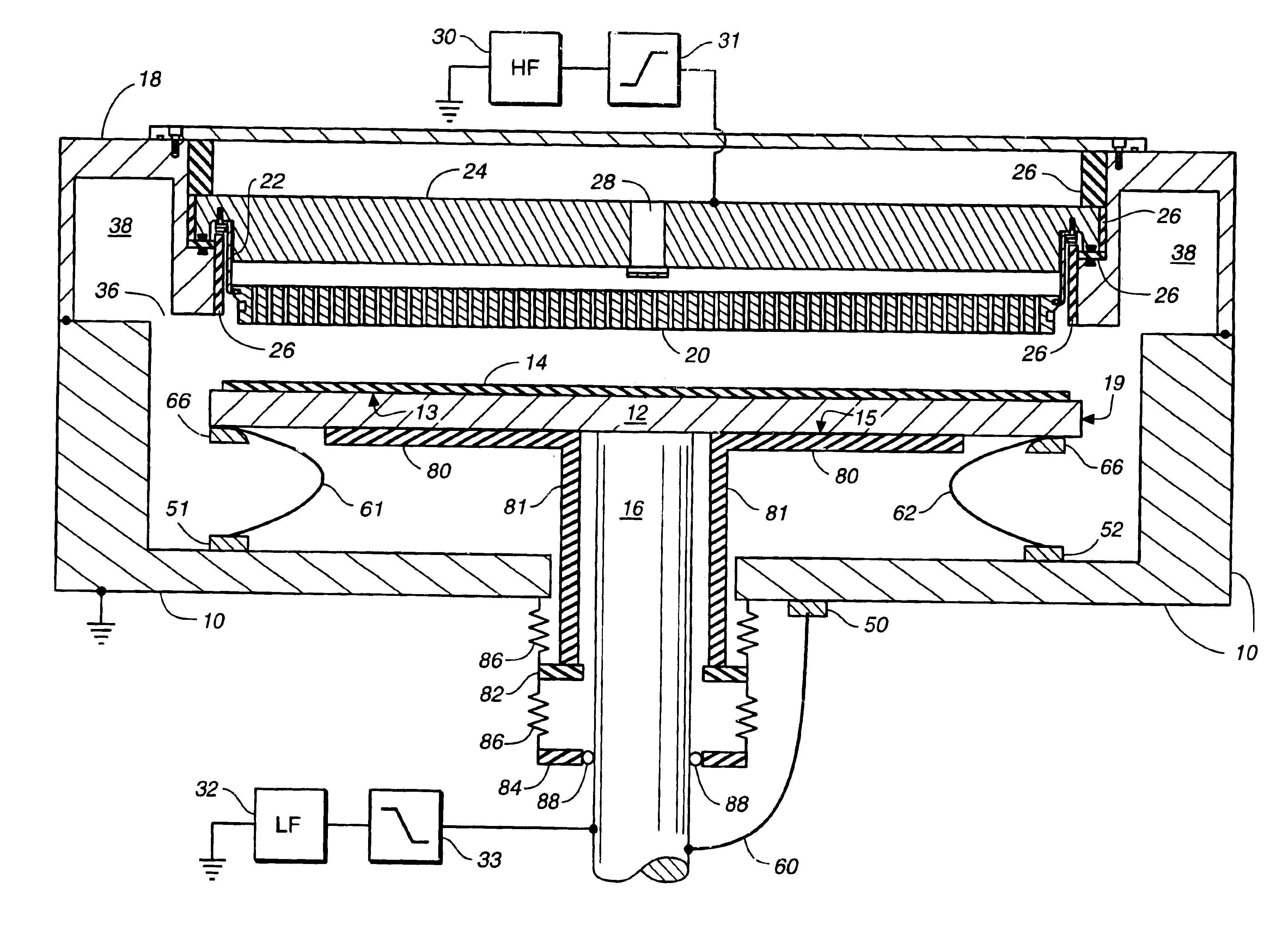
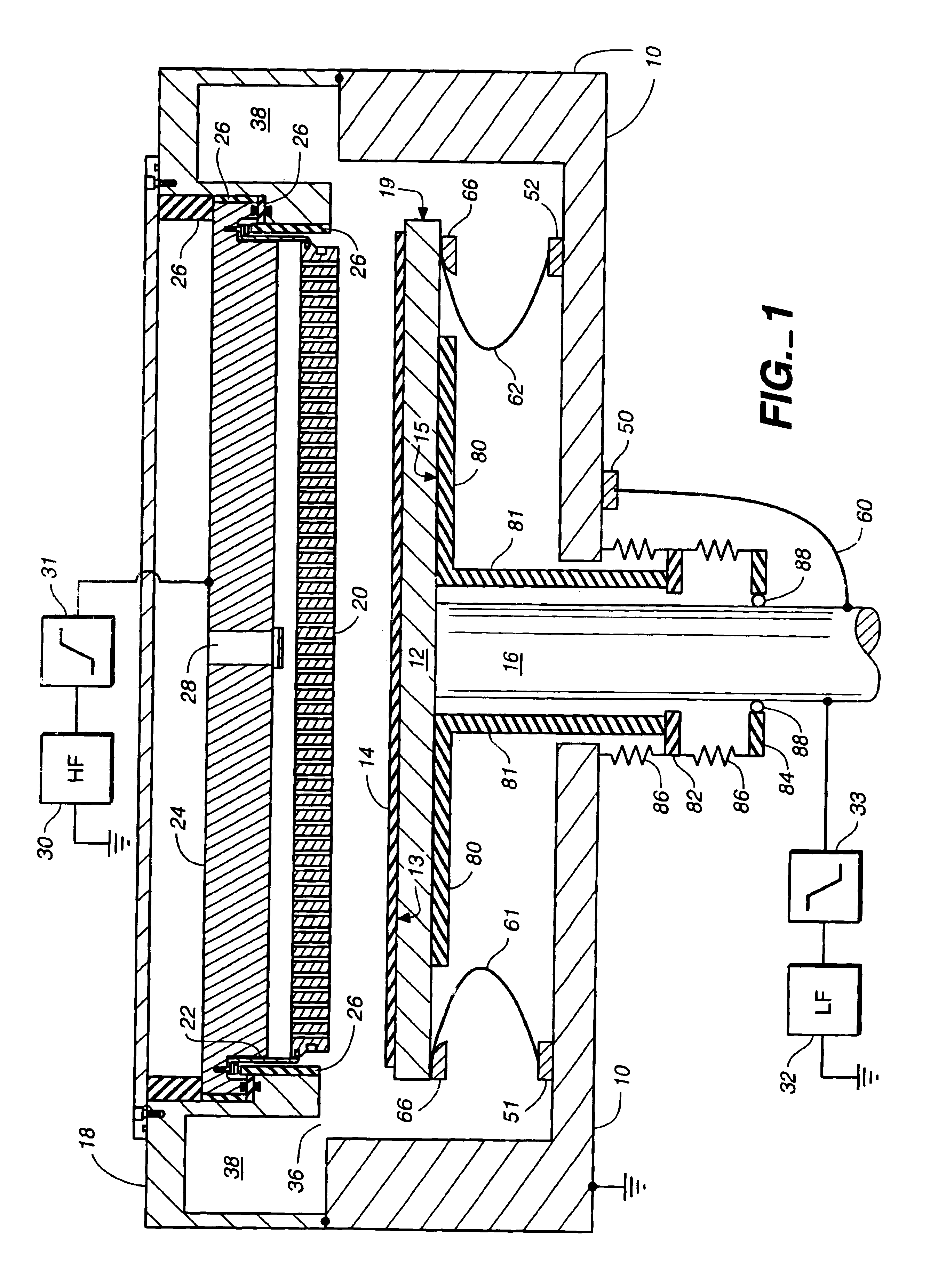
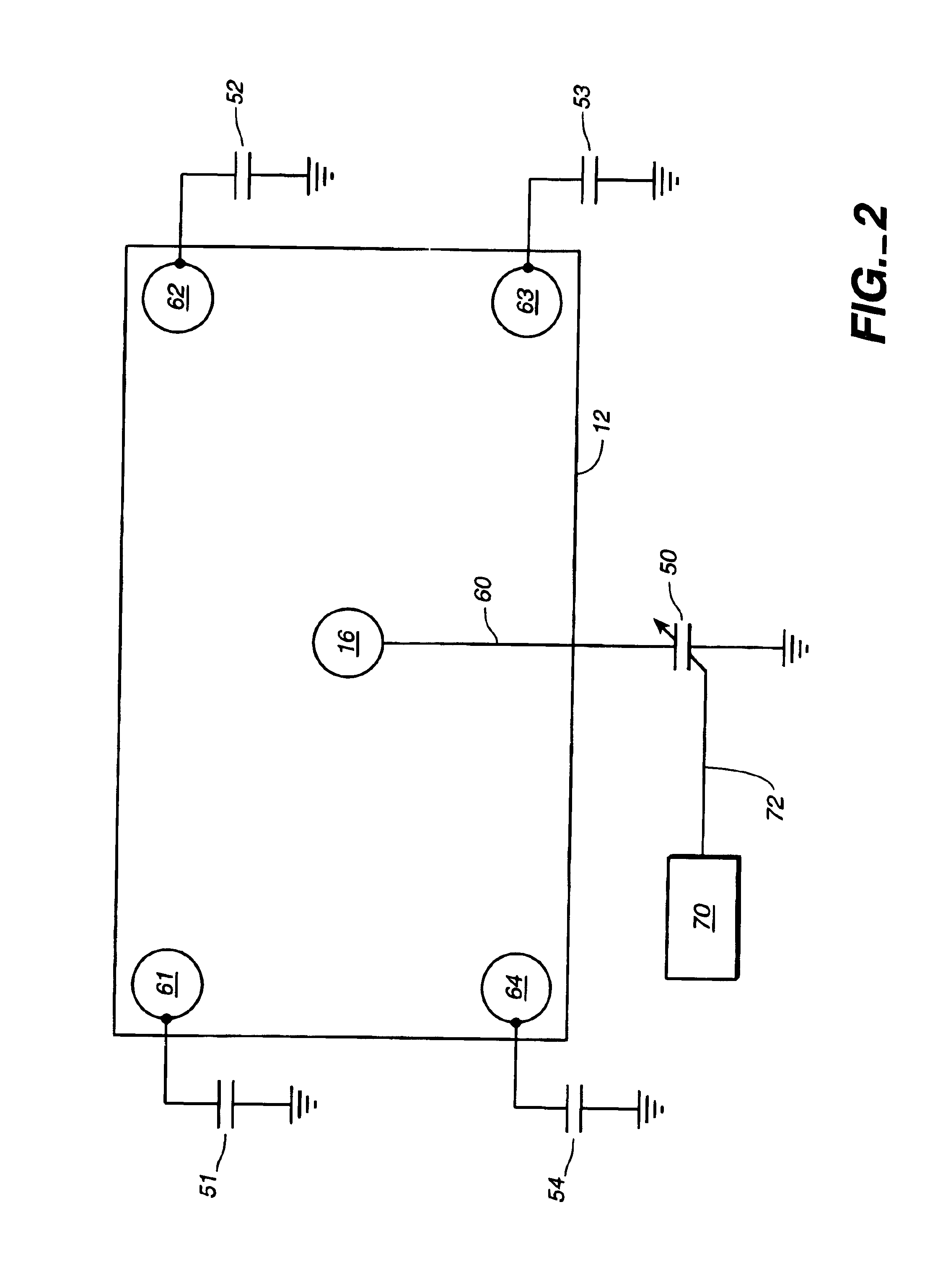
FIG. 1 shows a plasma chamber that includes capacitors connected between the cathode electrode and ground according to the present invention. The conventional features of the chamber will be described before describing the details of our invention.

The invention is useful in plasma chambers for fabricating or treating any kind of electronic substrate or workpiece, such as a silicon wafer or a glass substrate for a flat panel display. The illustrated chamber is designed for performing plasma-enhanced chemical vapor deposition (CVD) of films onto glass substrates. However, the invention also is useful in chambers for performing other plasma-assisted processes such as plasma etching.

The plasma chamber or vacuum chamber has a housing or wall 10 that encloses the side and bottom of the chamber interior and is electrically grounded. A metal pedestal or susceptor 12 functions as a cathode electrode and has a front surface 13 that supports a workpiece or substrate 14. We refer ...


PUM

PropertyMeasurementUnit
thickaaaaaaaaaa
frequenciesaaaaaaaaaa

Abstract

An apparatus and method for fabricating an electronic workpiece in which first and second electrodes within a plasma chamber are respectively connected to low frequency and high frequency RF power supplies. At least one capacitor is connected between the first electrode and electrical ground. The one or more capacitors can reduce or eliminate the coupling of high frequency RF power to any plasma outside the region directly between the two electrodes. Consequently, the invention can improve the performance of the plasma process by concentrating more of the RF power in the region between the two electrodes.

Description

FIELD OF THE INVENTIONThe invention relates generally to plasma chambers for fabricating electronic substrates in which the plasma is excited by RF power applied between anode and cathode electrodes. More specifically, the invention relates to such a chamber in which the anode and cathode receive RF power at different frequencies, and a capacitor is connected between the cathode electrode and electrical ground.BACKGROUND OF THE INVENTIONElectronic devices, such as flat panel displays and integrated circuits, commonly are fabricated by a series of process steps in which layers are deposited on a substrate and the deposited material is etched into desired patterns. The process steps commonly include plasma enhanced chemical vapor deposition (CVD) processes and plasma etch processes.Plasma processes require supplying a process gas mixture to a vacuum chamber called a plasma chamber, and then applying electrical or electromagnetic power to excite the process gas to a plasma state. The p...

Claims


Application Information

Patent Timeline
Patent Type & Authority Patents(United States)
IPC IPC(8): H01J37/32H05H1/46B01J19/08C23C16/34C23C16/509C23C16/52H01L21/302H01L21/3065H01L21/31
CPCC23C16/345C23C16/5096H01J37/32165H01J37/32082C23C16/52
Inventor SUN, SHENGOLSEN, JEFF C.YADAV, SANJAYSHANG, QUANYUANLAW, KAM S.
Owner APPLIED MATERIALS INC
Why Eureka
Try Eureka