Method and apparatus for a dynamically self-bootstrapped switch

a dynamically self-bootstrapped, switch technology, applied in the field of switches, can solve the problems of limiting the bandwidth of the switch, affecting the operation of the switch, and the transistor may have large parasitic capacitances, so as to reduce the coupling or elimination of the coupling voltage, short out the resistors of the circuit, and reduce the effect of signal loss

Active Publication Date: 2011-04-19
ANALOG DEVICES INC
View PDF37 Cites 35 Cited by
  • Summary
  • Abstract
  • Description
  • Claims
  • Application Information

AI Technical Summary

Benefits of technology

[0007]A circuit in accordance with one embodiment of the present invention connects resistors in series with the control node(s) of a switch, and, by placing bypass switches in parallel with the resistors, may selectively short out the resistors from the circuit. This system and method of dynamic self-bootstrapping disables the bypass switches when the switch is in an on-state, allowing the resistors to self-bootstrap the switch, and enables the bypass switches when the switch is in an off-state. The bypass switches thereby reduce or eliminate the coupling of the voltage at the input of the switch to the control node(s) when the switch is in an off-state. The circuit therefore reduces signal loss and improves the signal bandwidth and linearity of the switch, while also maintaining the off-state isolation of the switch.
[0012]In general, in a second aspect, a method of dynamically self-bootstrapping a switch includes connecting a first resistor between a control node of the switch and a switch control input. A voltage on the control node is allowed to track an input signal voltage when the switch is in an on-state. The voltage on the control node is prevented from tracking the input signal voltage when the switch is in an off-state by bypassing the first resistor with a first bypass switch.

Problems solved by technology

This FET switch may exhibit poor performance at high frequencies, such as RF frequencies.
At this size, however, the transistor may have large parasitic capacitances connecting the source and drain to the transistor's gate and back gate.
At high frequencies, the gate and back gate may have low impedances, and the parasitic capacitors may short the switch's input signal to these low impedance nodes and thereby limit the bandwidth of the switch.
Furthermore, a varying signal applied to the transistor's input may modulate the conductance (Gds) of the transistor, which may produce intermodulation distortion (“IMD”) and reduce the linearity of the switch.
Thus, while the resistors may reduce the on-state loss of the switch, they also undesirably affect the off-state isolation of the switch.

Method used


Image

  • Method and apparatus for a dynamically self-bootstrapped switch
  • Method and apparatus for a dynamically self-bootstrapped switch
  • Method and apparatus for a dynamically self-bootstrapped switch

Examples


Embodiment Construction

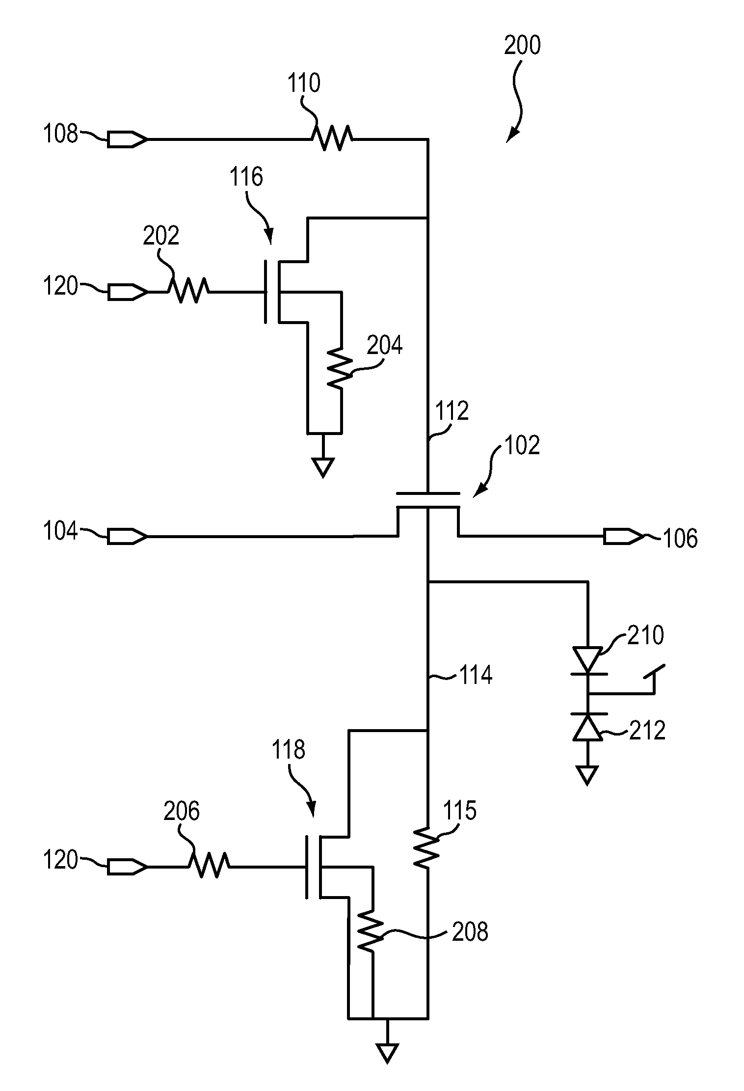
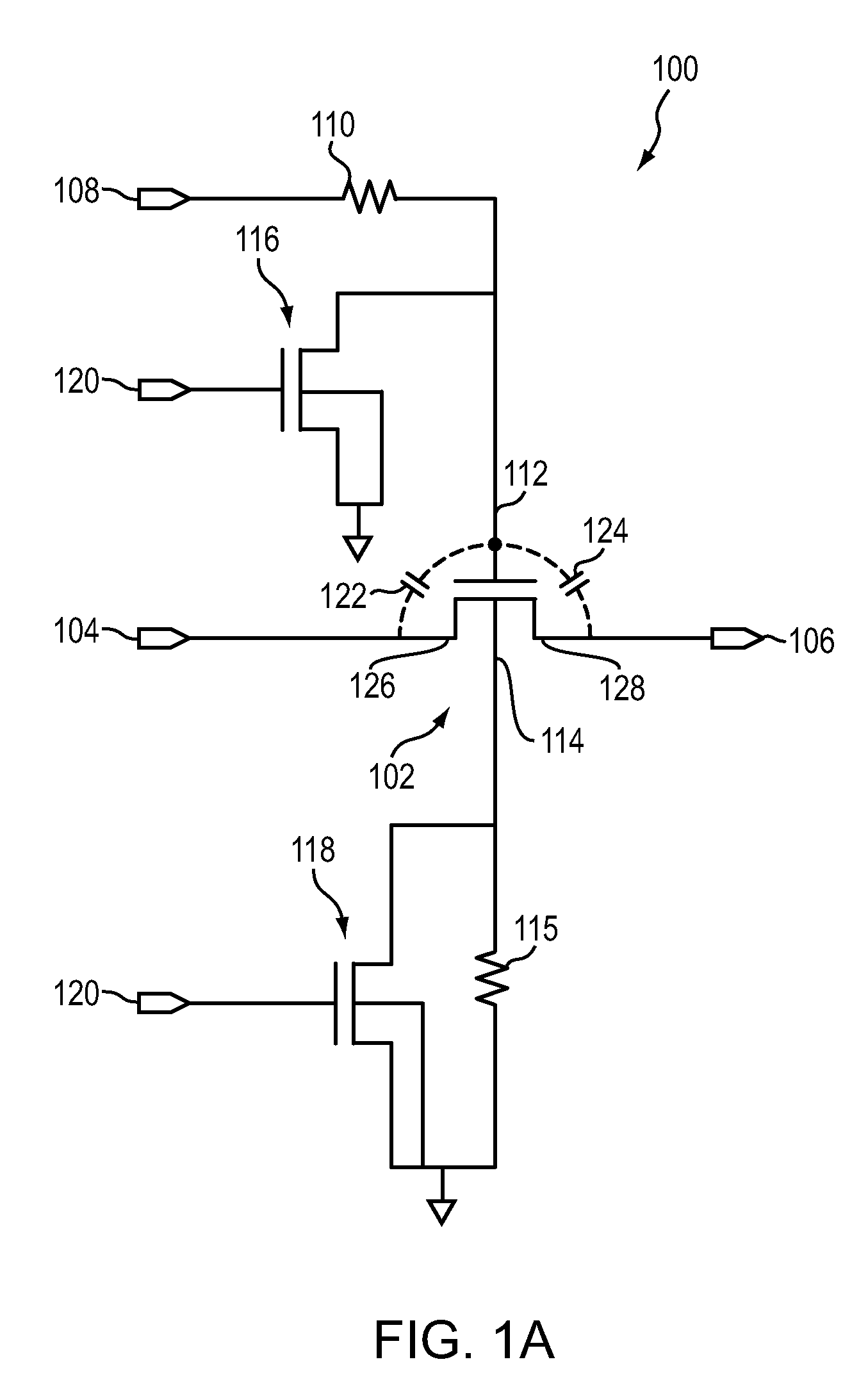
[0026]In general, the present invention pertains, in various embodiments, to devices, systems, and methods for dynamically self-bootstrapping a switch. To provide an overall understanding of the invention, certain illustrative embodiments are described, including devices, systems, and methods for dynamically self-bootstrapping a MEMS switch and an NMOS pass-gate switch by using control node resistors and bypass switches.

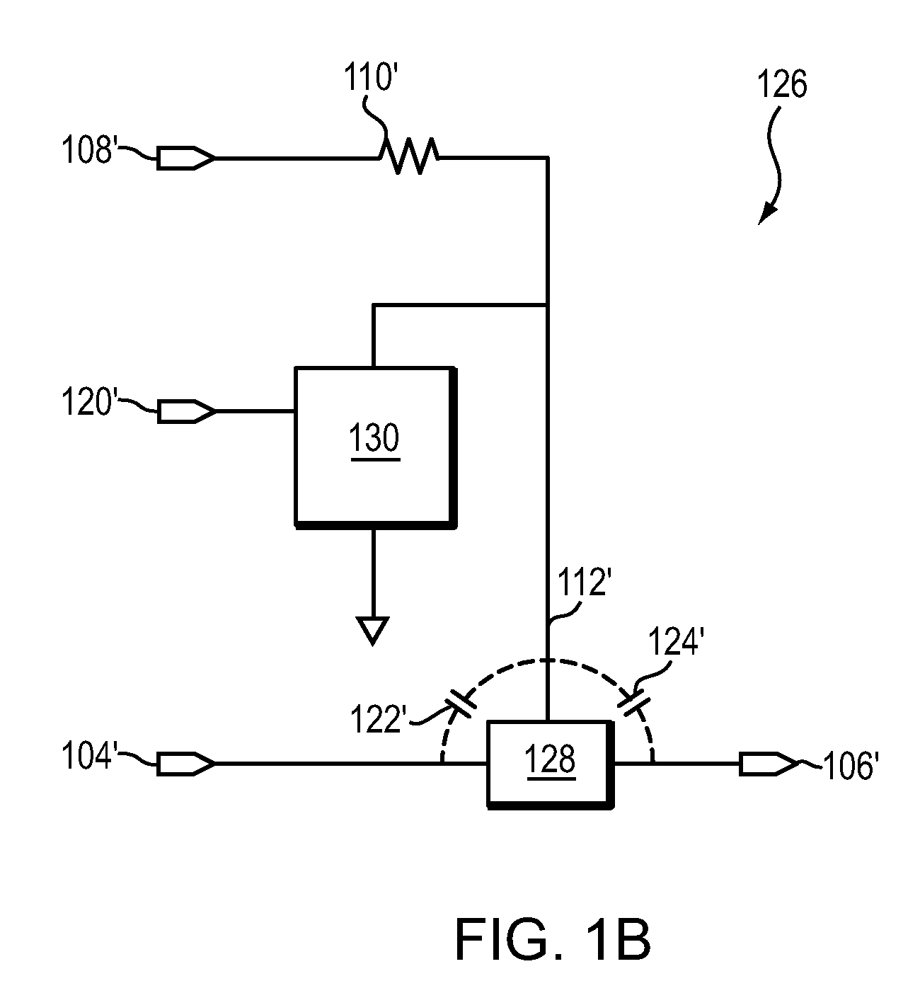
[0027]FIG. 1A illustrates a circuit 100 in accordance with one embodiment of the present invention. The circuit 100 features an NMOS pass-gate transistor 102 with a signal input 104, an output 106, and a switch control input 108. One of skill in the art will understand that a pass-gate switch is but one possible implementation of a FET switch, and that many other implementations exist. For example, the pass-gate switch may alternatively feature a PMOS transistor, or NMOS and PMOS transistors in parallel. A gate resistor 110 is in series with the gate 112, and a back-...


PUM


Abstract

A dynamically self-bootstrapping circuit for a switch features a resistor in series with the control node of the switch. A bypass switch connects a control node to ground. When the switch is in an off-state, the bypass switch is enabled.

Description

TECHNICAL FIELD[0001]The present invention relates, in various embodiments, to switches and systems and methods of dynamically self-bootstrapping the same.BACKGROUND[0002]Switches, such as field-effect transistor (“FET”) or micro-electro-mechanical system (“MEMS”) switches, are used extensively in analog, mixed-signal, and radio-frequency (“RF”) applications. RF applications may use switches for signal routing (e.g., as transmit / receive switches), as switched attenuators, switched resonators, switched capacitors, or as capacitor band-switched voltage-controlled oscillators (“VCO”). A switch may also be used as, for example, a mixer.[0003]One example of a FET switch is an n-type metal-oxide-semiconductor (“NMOS”) transistor pass-gate, wherein the input signal is received at the transistor's source, the output is generated by the transistor's drain, and the gate and back gate of the transistor control the state of the switch.[0004]This FET switch may exhibit poor performance at high f...

Claims


Application Information

Patent Timeline
Patent Type & Authority Patents(United States)
IPC IPC(8): H03K17/687
CPCH03K17/04106H01H59/0009H03K2217/0018
Inventor BALBONI, EDMUND J.
Owner ANALOG DEVICES INC
Why Eureka
Try Eureka