
Quantum dots of group IV semiconductor materials

a semiconductor material and quantum dots technology, applied in the field of quantum dots, can solve the problems of low yield, increase in energy gap, lack of reproducibility, etc., and achieve the effect of decreasing the overall fom, increasing optical losses, and negative impact on performan

Inactive Publication Date: 2008-04-15
SAMSUNG ELECTRONICS CO LTD
View PDF174 Cites 84 Cited by
  • Summary
  • Abstract
  • Description
  • Claims
  • Application Information

AI Technical Summary

Benefits of technology

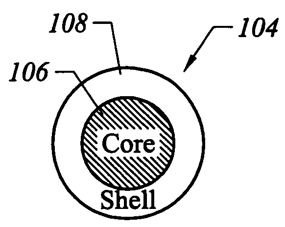
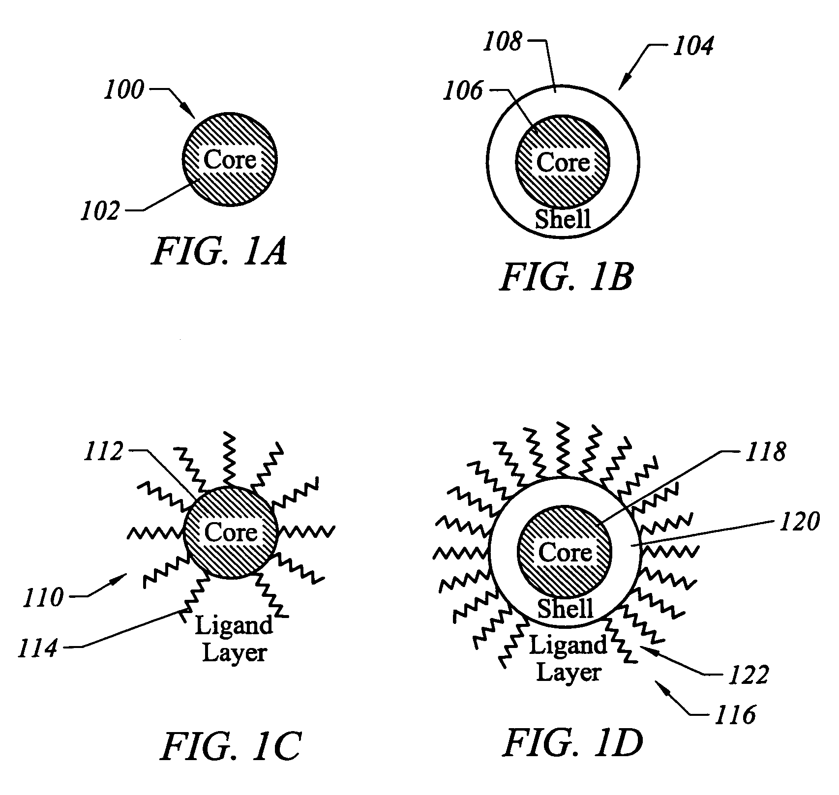
The present invention is about a new type of quantum dot that has a core made of semiconductor material (Si or Ge) and a shell made of a different material. The quantum dot is defect-free, meaning it has no defects that would affect its performance. The quantum dot also has a ligand layer that includes surface ligands. This new quantum dot has a high quantum efficiency, meaning it can produce light with high efficiency.

Problems solved by technology

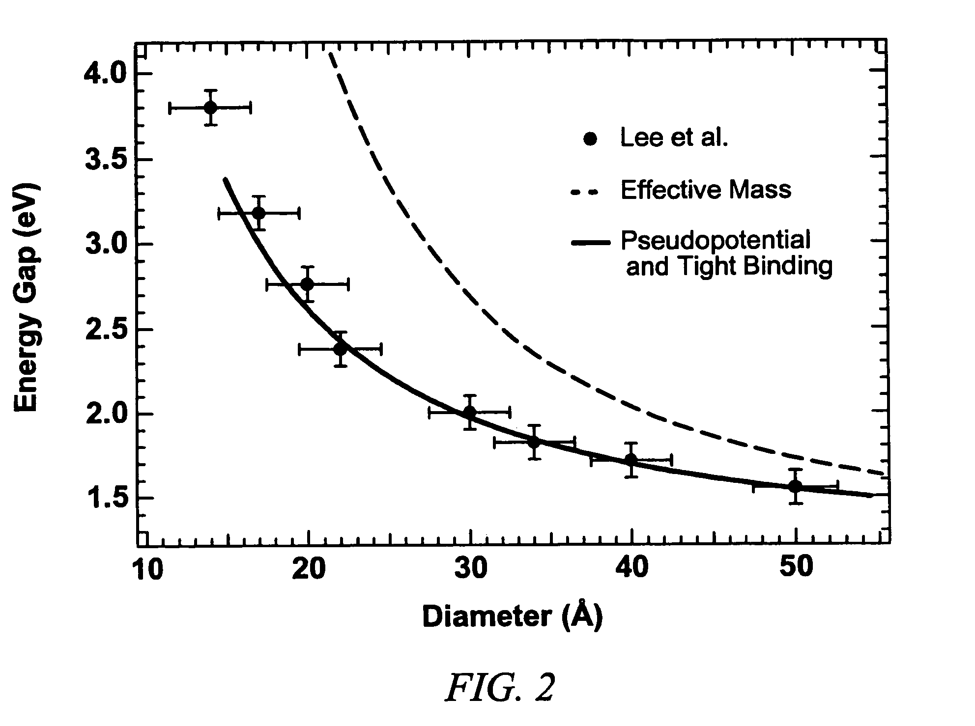
For instance, quantum confinement effects can lead to an increase in energy gap as the size of the quantum dots is decreased.
In particular, formation of quantum dots of Si or Ge sometimes involved extreme conditions of temperature and pressure while suffering from low yields and lack of reproducibility.
And, quantum dots that were produced were generally incapable of exhibiting adequate levels of photoluminescence that can be tuned over a broad spectral range.
Also, previous attempts have generally been unsuccessful in producing quantum dots of Si or Ge that are sufficiently stable under ambient conditions or that can be made sufficiently soluble in a variety of matrix materials.

Method used


Image

  • Quantum dots of group IV semiconductor materials
  • Quantum dots of group IV semiconductor materials
  • Quantum dots of group IV semiconductor materials

Examples


example 1

[0242]A 500-ml three-neck round bottom flask equipped with a stirring bar, a reflux condenser, and a thermometer was purged with argon and charged with 200 ml of the selected solvent (e.g., glymes (n=1 to 5)) and the reducing agent (e.g., magnesium powder, 0.05 to 0.20 mol). Freshly distilled YX4 (0.05 to 0.20 mol) was added dropwise, and the resulting brown-reddish solution was heated to higher temperatures (e.g., between approximately 60 and 280° C.) for a period of time (e.g., between approximately 2 and 100 hrs, typically between approximately 2 and 48 hrs). The resulting mixture was cooled to about −20° C. and treated with an excess amount of the capping agent (e.g., 1.8 M solution of phenyllithium), which was added dropwise to keep the temperature below room temperature. After the reaction mixture was stirred at ambient temperature for a period of time (e.g., between approximately 2 and 48 hrs), it was quenched with dilute protic acid (pH˜2) and extracted with an organic solve...

example 2

[0243]The preparation of Example 1 is repeated using sodium as the reducing agent.

example 3

[0244]The preparation of Example 1 is repeated using barium as the reducing agent.


PUM

PropertyMeasurementUnit
quantum efficiencyaaaaaaaaaa
diameteraaaaaaaaaa

Abstract

The invention relates to a quantum dot. The quantum dot comprises a core including a semiconductor material Y selected from the group consisting of Si and Ge. The quantum dot also comprises a shell surrounding the core. The quantum dot is substantially defect free such that the quantum dot exhibits photoluminescence with a quantum efficiency that is greater than 10 percent.

Description

CROSS-REFERENCE TO RELATED APPLICATIONS[0001]This application is a divisional of U.S. patent application Ser. No. 10 / 212,001, filed on Aug. 2, 2002 now abandoned, which claims the benefit of U.S. Provisional Application Ser. No. 60 / 309,898, filed on Aug. 2, 2001, U.S. Provisional Application Ser. No. 60 / 309,905, filed on Aug. 2, 2001, U.S. Provisional Application Ser. No. 60 / 309,979, filed on Aug. 2, 2001, U.S. Provisional Application Ser. No. 60 / 310,090, filed on Aug. 2, 2001, and U.S. Provisional Application Ser. No. 60 / 310,095, filed on Aug. 2, 2001, the disclosures of which are incorporated herein by reference in their entirety.FIELD OF THE INVENTION[0002]This invention relates generally to quantum dots. More particularly, this invention relates to quantum dots of Group IV semiconductor materials.BACKGROUND OF THE INVENTION[0003]Over the past several years, there has been an increasing interest in exploiting the extraordinary properties associated with quantum dots. As a result ...

Claims


Application Information

Patent Timeline
Patent Type & Authority Patents(United States)
IPC IPC(8): H01L31/028G02B6/12G02B6/122G02F1/017G02F1/35G02F1/355G02F1/365G02F2/00H01L21/20H01L29/12H01L29/16H01L33/20H01L33/34
CPCB82Y10/00G02B6/122G02B6/1225G02F1/3515G02F1/3556H01L29/127B82Y20/00Y10S977/814G02B2006/12097G02B2006/12145G02B2006/12147G02B2006/12159G02B2006/12195G02F1/3517G02F1/3521G02F1/365G02F2001/01791G02F2001/217G02F2002/006G02F2202/32G02F2202/36H01L29/16H01L29/1602H01L33/20H01L33/34G02F1/01791G02F1/217G02F2/006
Inventor LEE, HOWARD WING HOON
Owner SAMSUNG ELECTRONICS CO LTD
Learn More