Nanophotovoltaic Device with Improved Quantum Efficiency

a photovoltaic and quantum efficiency technology, applied in the field of photovoltaic devices, can solve the problems of high cost of silicon solar cells, inability to achieve significant cost reduction, and mature manufacturing,

Inactive Publication Date: 2008-06-19
SOLEXANT
View PDF48 Cites 82 Cited by
  • Summary
  • Abstract
  • Description
  • Claims
  • Application Information

AI Technical Summary

Benefits of technology

[0017]In one embodiment, the photovoltaic device comprises first and second electrodes, at least one of which is a transparent electrode that is substantially transparent to all or part of the solar spectrum. A photoactive layer is disposed between the first and second electrodes. The photoactive layer comprises a firs...

Problems solved by technology

Silicon solar cells are very expensive.
Manufacturing is mature and not amenable for significant cost reduction.
Silicon is not an ideal material for use in solar cells as it primarily absorbs in the visible region of the solar spectrum thereby limiting the conversion efficiency.
But by the end of that decade, and in the early 1990s, it was dismissed by many observers for its low efficiencies and instability.
The key obstacles to a-Si technology are low efficiencies (about 11% stable), light-induced efficiency degradation (which requires more complicated cell designs such as multiple junctions), and process costs (fabrication methods are vacuum-based and fairly slow).
These record breaking small area devices have been fabricated using vacuum evaporation techniques which are capital intensive and quite costly.
It is very challenging to fabricate CIGS films of uniform composition on large area substrates.
This limitation also affects the process yield, which are generally quite low.
Because of these limitations, implementation of evaporation techniques has not been successful for large-scale, low-cost commercial production of thin f...

Method used


Image

  • Nanophotovoltaic Device with Improved Quantum Efficiency
  • Nanophotovoltaic Device with Improved Quantum Efficiency
  • Nanophotovoltaic Device with Improved Quantum Efficiency

Examples


example 1

Preparation

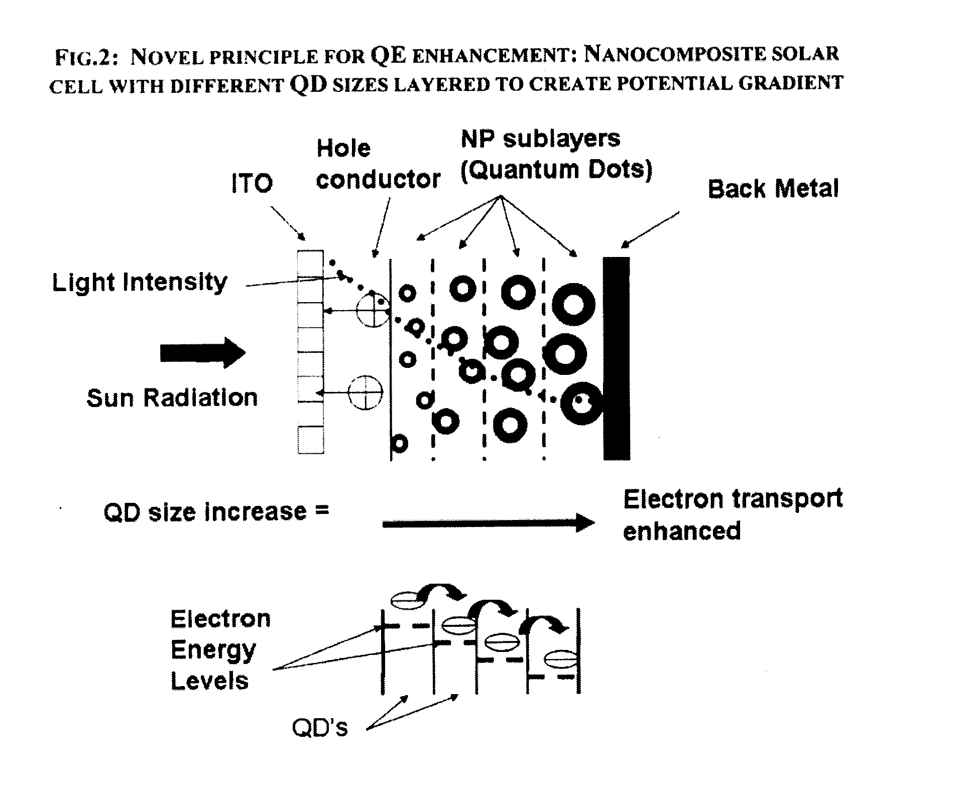
[0090]In the embodiment shown in FIG. 4 the photoactive layer is a nanocomposite film with three sublayers of quantum dots and a hole conducting sublayer. The quantum dots in each of the sublayers have essentially the same size but have different compositions. The sublayers are arranged in such a way that the quantum dots with the largest bandgap are located closer to the first electrode while the quantum dots with smallest bandgap are located closer to the second electrode (the Back Metal region). The respective sub-layer thickness and the number of sub-layers depend on the total film thickness and the number of quantum dot material grades. For instance for the 150 nm thick nanocomposite film with different types of quantum dot materials, the approximate sub-layer thickness will be in the 25-30 nm range. The approximate light absorption trend is also shown in FIG. 4. Due to the different energy quantization in quantum dots of different size the longer wavelength absorpti...

example 2

[0091]In the embodiment shown in FIG. 3 the quantum dots in the nanocomposite film (photoactive layer) are made up of three elements, and the quantum dots are arranged such that the smallest quantum dots are located closer to the first electrode while the biggest quantum dots are located closer to the second electrode (the Back Metal region). The bandgap of the quantum dots also varies inversely with size (the smallest quantum dot has the largest bandgap). The respective sub-layer thickness and the number of sub-layers depend on the total nanocomposite film thickness and the number of types of quantum dots. For instance for the 150 nm thick nanocomposite film and nanoparticle size varying from 3 to 9 nm the approximate sub-layer thickness will be in the 15-25 nm range. The approximate light absorption trend is also shown in FIG. 3. Apparently due to the different energy quantization in quantum dots of different size the longer wavelength absorption is expected to shift toward the fa...

example 3

[0092]In the embodiment shown in FIG. 5 the quantum dots in the sublayers of the nanocomposite film (photoactive layer) are arranged such that the smallest quantum dots are located closer to the first electrode while the biggest quantum dots are located closer to the second electrode (the Back Metal region). The bandgap of the quantum dots also varies inversely with size (the smallest quantum dot has the largest bandgap). The different colors of the quantum dots in each level correspond to their different compositions. The respective sub-layer thickness and the number of sub-layers depend on the total nanocomposite film thickness and the number of types of quantum dots. For instance for the 150 nm thick nanocomposite film and nanoparticle size varying from 3 to 9 nm the approximate sub-layer thickness will be in the 15-25 nm range. The approximate light absorption trend is also shown in FIG. 3. Apparently due to the different energy quantization in quantum dots of different size the...


PUM


Abstract

Photovoltaic devices or solar cells are provided having one or more photoactive layers where at least one of the photoactive layers comprises a sublayer made of photoactive nanoparticles that differ in size, composition or both.

Description

RELATED APPLICATION[0001]This patent application claims the benefit of, and priority to, U.S. Provisional Patent Application Ser. No. 60 / 873,139 filed on Dec. 6, 2006, titled “NanoMaterial Solar Cell with the Enhanced PV Quantum Efficiency,” the disclosure of which is hereby incorporated by reference in its entirety.FIELD OF THE INVENTION[0002]In general, the present invention relates to the field of photovoltaics or solar cells. More particularly, the present invention relates to photovoltaic devices having photoactive layers made of sublayers of photoactive nanoparticles.BACKGROUND OF THE INVENTION[0003]Increasing oil prices have heightened the importance of developing cost effective renewable energy. Significant efforts are underway around the world to develop cost effective solar cells to harvest solar energy. Current solar energy technologies can be broadly categorized as crystalline silicon and thin film technologies. More than 90% of the solar cells are made from silicon—sing...

Claims


Application Information

Patent Timeline
IPC IPC(8): H01L31/0224
CPCB82Y20/00H01L31/0352Y02E10/50H01L31/078H01L31/035236
Inventor REDDY, DAMODERGILMAN, BORIS
Owner SOLEXANT
Why Eureka
Try Eureka