Semiconductor device provided with matrix type current load driving circuits, and driving method thereof

a technology of current load driving circuit and semiconductor device, which is applied in the direction of semiconductor device, electrical apparatus, instruments, etc., can solve the problems of large current flow, passive driving device consumes a measurable amount of power, and active driving device consumes less power

Active Publication Date: 2005-07-07
HANNSTAR DISPLAY CORPORATION
View PDF9 Cites 227 Cited by
  • Summary
  • Abstract
  • Description
  • Claims
  • Application Information

AI Technical Summary

Benefits of technology

[0027] In accordance with yet another aspect of the present invention, there is provided a method for driving a semiconductor device that performs active drive current programming and comprises current load cells each having a current load and a current load driving circuit, which are arranged in a matrix, wherein: the output of a current driver for current-driving data lines is input in a selector; the selector selects the plural data lines connected respectively to the outputs of the selector one by one based on an output select signal input therein; the output of the current driver is supplied to the selected data line; the current load driving circuit in each of the current load cells includes a transistor whose source is connected to a first power supply while whose drain is connected to the current load directly or via a switch for supplying current to the current load, a capacitance connected between the gate of the transistor and the first power supply or another power supply, and a switch or a plurality of series-connected switches connected between the gate of the transistor and a corresponding data line; and there are control lines, each of which transmits a signal for controlling the switch in the current load driving circuit, at least as many as data lines selectable by one current output of the current driver in one line of the semiconductor device; comprising: a first step for passing current corresponding to the current output supplied from the current driver to the selected data line through the transistor in the current load cell, and setting a voltage that causes the current to flow in the gate of the transistor and the capacitance by turning on the switch whose one end is connected to the gate of the transistor in the current load cell with a control signal transmitted through one of the plural control lines corresponding to the selected data line during the period while the selector selects one of the plural data lines based on the output select signal in one horizontal period for selecting one line; and a second step for turning off the switch before or upon completion of the select period for the selected data line; wherein the first and second steps are performed with respect to each of the plural data lines to complete current programming for the current load cells corresponding to one line.
[0028] In accordance with yet another aspect of the present invention, there is provided a method for driving a semiconductor device that performs active drive current programming, and comprises: current load cells each having a current load and a current load driving circuit, which are arranged in a matrix; and a means for selecting a plurality of data lines one by one to supply the current output of a current driver for supplying current to the respective data lines; wherein: the current load driving circuit in each of the current load cells includes a transistor whose source is connected to a first power supply while whose drain is connected to the current load directly or via a switch for supplying current to the current load, a capacitance connected between the gate of the transistor and the first power supply or another power supply, and a plurality of switches connected in series between the gate of the transistor and a corresponding data line; there are control lines, each of which transmits a signal for controlling the switch whose one end is connected to the gate of the transistor included in the current load driving circuit, at least as many as data lines selectable for one output of the current driver in one line of the semiconductor device; and there are control lines, each of which transmits a signal for controlling the switch whose one end is connected to the data line corresponding to the current load cell having the current load driving circuit, in each line of the semiconductor device; comprising: a first step for setting the respective switches whose one ends are connected to the data lines corresponding to the current load cells for one line to the on state during one horizontal period with a control signal transmitted through the control line provided to each line in one horizontal period for selecting one line; a second step for passing current corresponding to the current output supplied from the current driver to the selected data line through the transistor in the current load cell, and setting a voltage that causes the current to flow in the gate of the transistor and the capacitance by turning on the switch whose one end is connected to the gate of the transistor in the current load cell with a control signal transmitted through one of the plural control lines corresponding to the selected data line during the period while the selector selects one of the plural data lines based on the output select signal; and a third step for turning off the switch before or upon completion of the select period for the selected data line; wherein the second and third steps are performed with respect to each of the plural data lines to complete current programming for the current load cells corresponding to one line.

Problems solved by technology

In the passive driving device, however, since the loads are driven only for a selected period of time, a large current flow is required.
Consequently, in the case of the passive driving device, the current loads 206 take heavy loads instantaneously, which may cause a problem with the reliability of elements that form the current loads 206.
Moreover, the passive driving device consumes a measurable amount of power because of a drop in efficiency.
In addition, the active driving device consumes lower amounts of power because of its high efficiency.
However, with the p-Si TFT, there are considerable variations in the current capacity of respective transistors, and therefore, it is highly likely that the driving current differs between TFTs even when the same voltage is used.
In this case, variations are produced in the brightness of the organic EL elements, and display accuracy deteriorates.
Consequently, it is necessary to provide the current drivers as many as all the data lines, which drives up costs.
In addition, there is another problem in that contact points between the current drivers and a device having current load cells for active drive arranged in a matrix increase, which reduces reliability and productivity.
In this case, however, yields, reliability and productivity decrease because the device as a whole increases in circuit size or scale as the circuit scale of current driver part becomes larger.

Method used


Image

  • Semiconductor device provided with matrix type current load driving circuits, and driving method thereof
  • Semiconductor device provided with matrix type current load driving circuits, and driving method thereof
  • Semiconductor device provided with matrix type current load driving circuits, and driving method thereof

Examples


embodiments

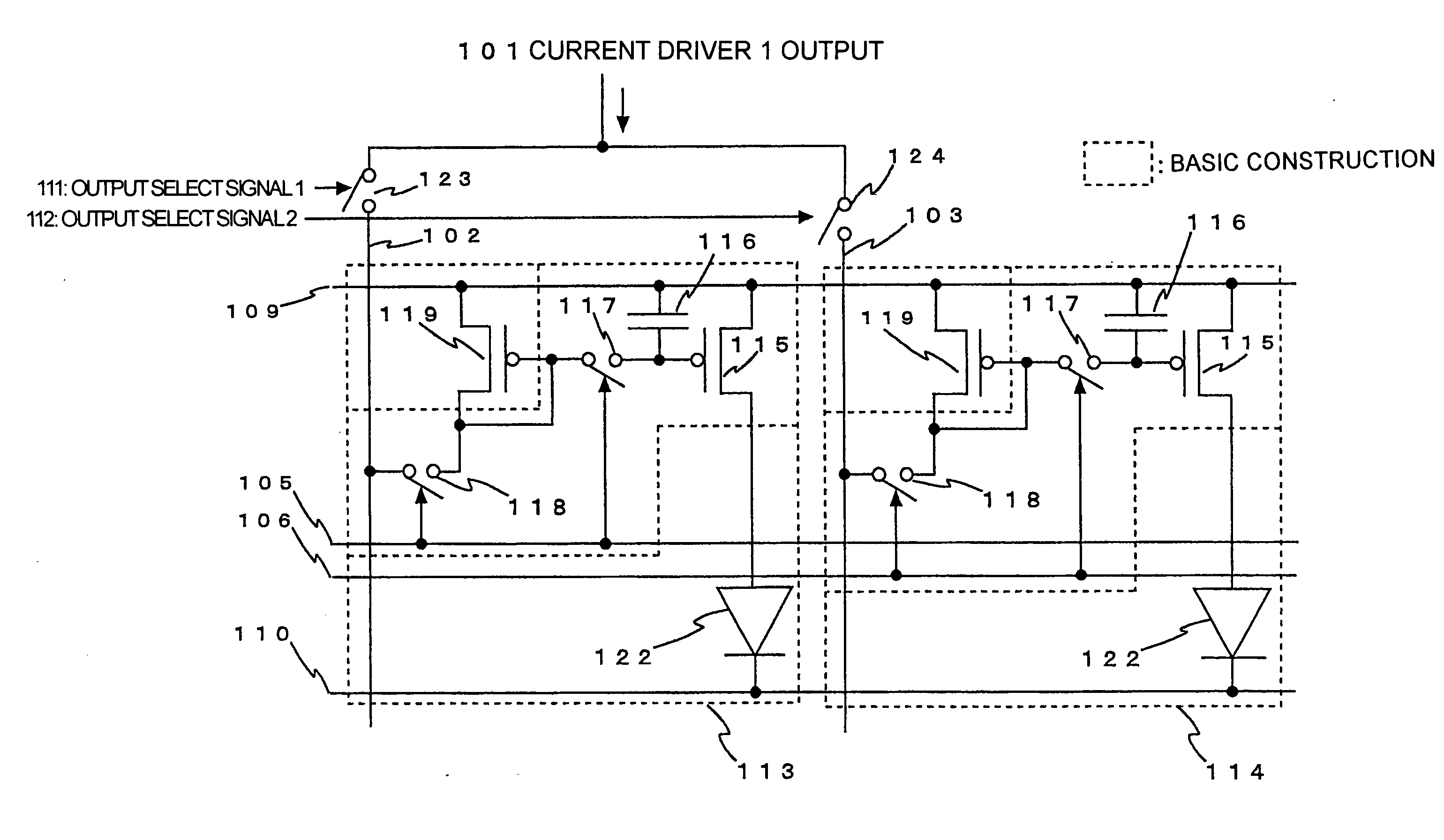
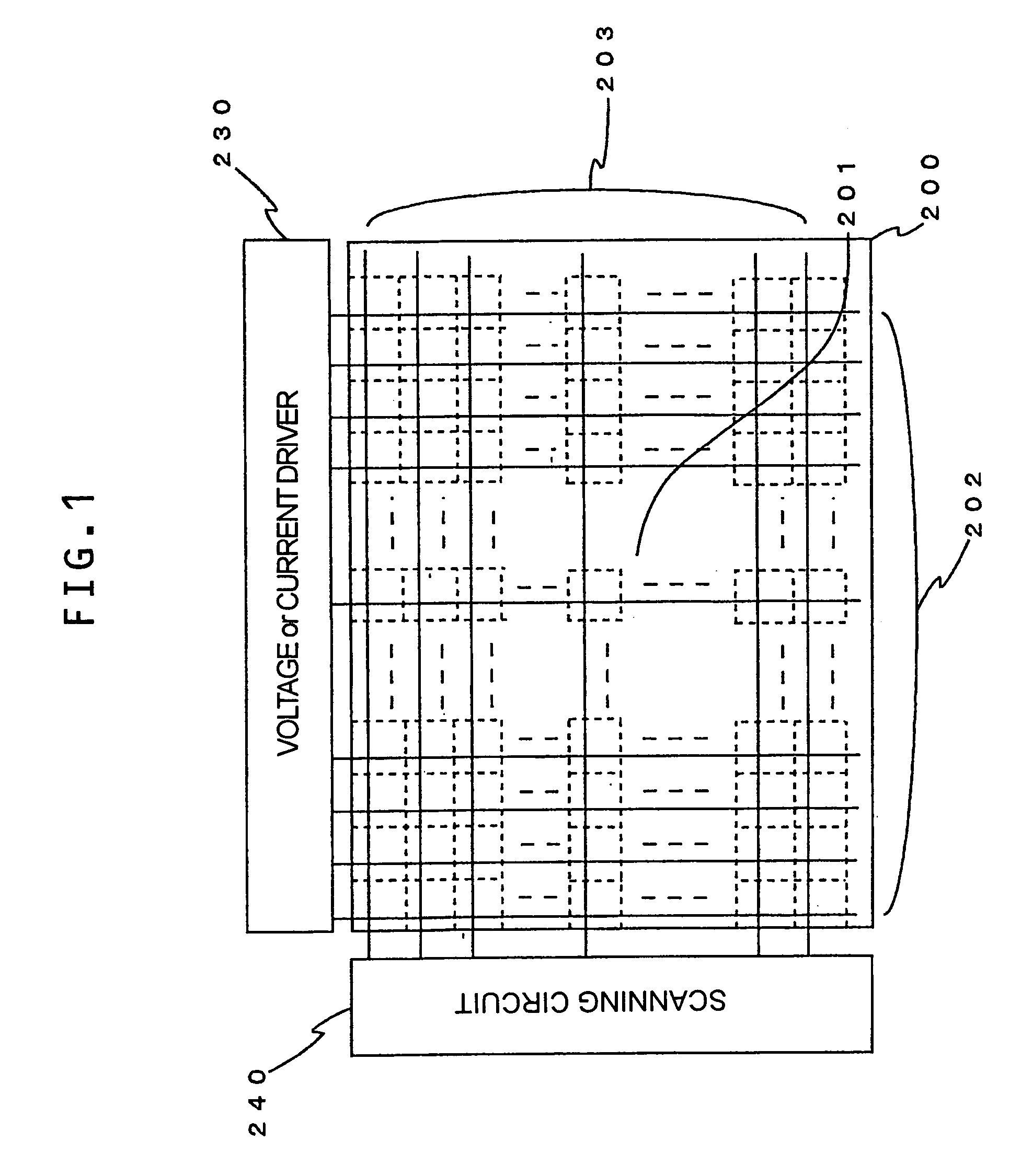
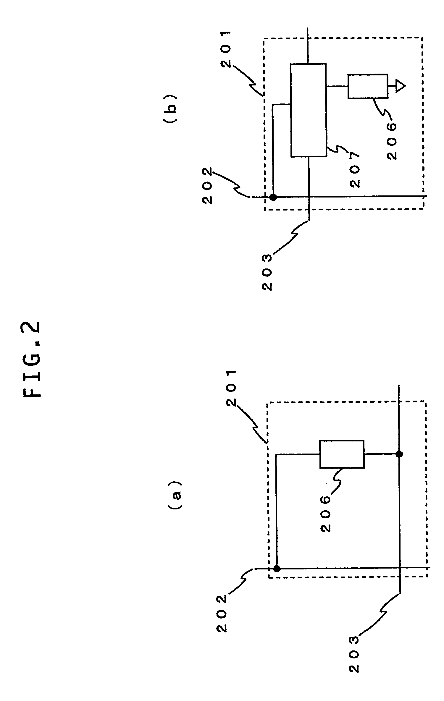
[0054] Referring now to the drawings, a description of the aforementioned embodiment of the present invention will be given in more detail. In the following, a light emitting display device using light emitting elements as the current loads will be described. Hereinafter, the current load cell will be referred to as a pixel, and the current load driving circuit will be referred to as a light emitting element driving circuit. However, the light emitting element is cited merely by way of example and without limitation. The present invention is applicable for driving any current load including specific one such as the organic EL element.

[0055]FIG. 5 is a diagram showing a circuitry according to the first embodiment of the present invention. Incidentally, while, in a schematic view of FIG. 5, one of the two data lines 102 and 103 is selected by the selector for one output 101 from the current driver, two or more data lines may be selected in the case, for example, where the driving tim...


PUM


Abstract

A semiconductor device to which active drive current programming is applied, comprising current load cells each having a current load and a current load driving circuit, which are arranged in a matrix, capable of reducing the circuit scale of a current driver with little change made in the structure of the current load driving circuit, and a driving method of the same.
A current load cell (113, 114) includes a current load driving circuit which is provided with a transistor (115) connected in series with a current load (122) between first and second power supplies (109, 110); a capacitance (116) connected between the control terminal of the transistor (115) and the first power supply (109); and switches (117, 118) connected between the control terminal of the transistor (115) and a corresponding data line. The output (101) of a current driver is connected to a plurality of data lines via a selector (123, 124), and the plural data lines connected to one output of the current driver via the selector and at least one of the switches of each of the current load cells corresponding to the respective data lines are drive-controlled in a time division manner during one horizontal period.

Description

TECHNICAL FIELD [0001] The present invention relates to a semiconductor device provided with current loads and current load driving circuits, and a driving method thereof, and more particularly, to a semiconductor device in which current loads and current load driving circuits are arranged in a matrix and an active drive is carried out, and a driving method of the same. BACKGROUND ART [0002]FIG. 1 is a diagram showing a known structure of a semiconductor device in which current loads are arranged in a matrix. The semiconductor device is finding various applications. In FIG. 1, a semiconductor device 200 comprises a plurality of data lines 202 in a parallel arrangement, a plurality of scanning lines 203 in a parallel arrangement running in a direction perpendicular to the data lines 202, and a matrix of current load cells 201 set at the intersections of the data lines 202 and scanning lines 203, respectively. The data lines 202 are voltage-driven or current-driven by a voltage driver...

Claims


Application Information

Patent Timeline
Patent Type & Authority Applications(United States)
IPC IPC(8): G09G3/32
CPCG09G3/3241G09G2310/0297G09G2300/0861G09G2300/0842
Inventor ABE, KATSUMI
Owner HANNSTAR DISPLAY CORPORATION
Why Eureka
Try Eureka