

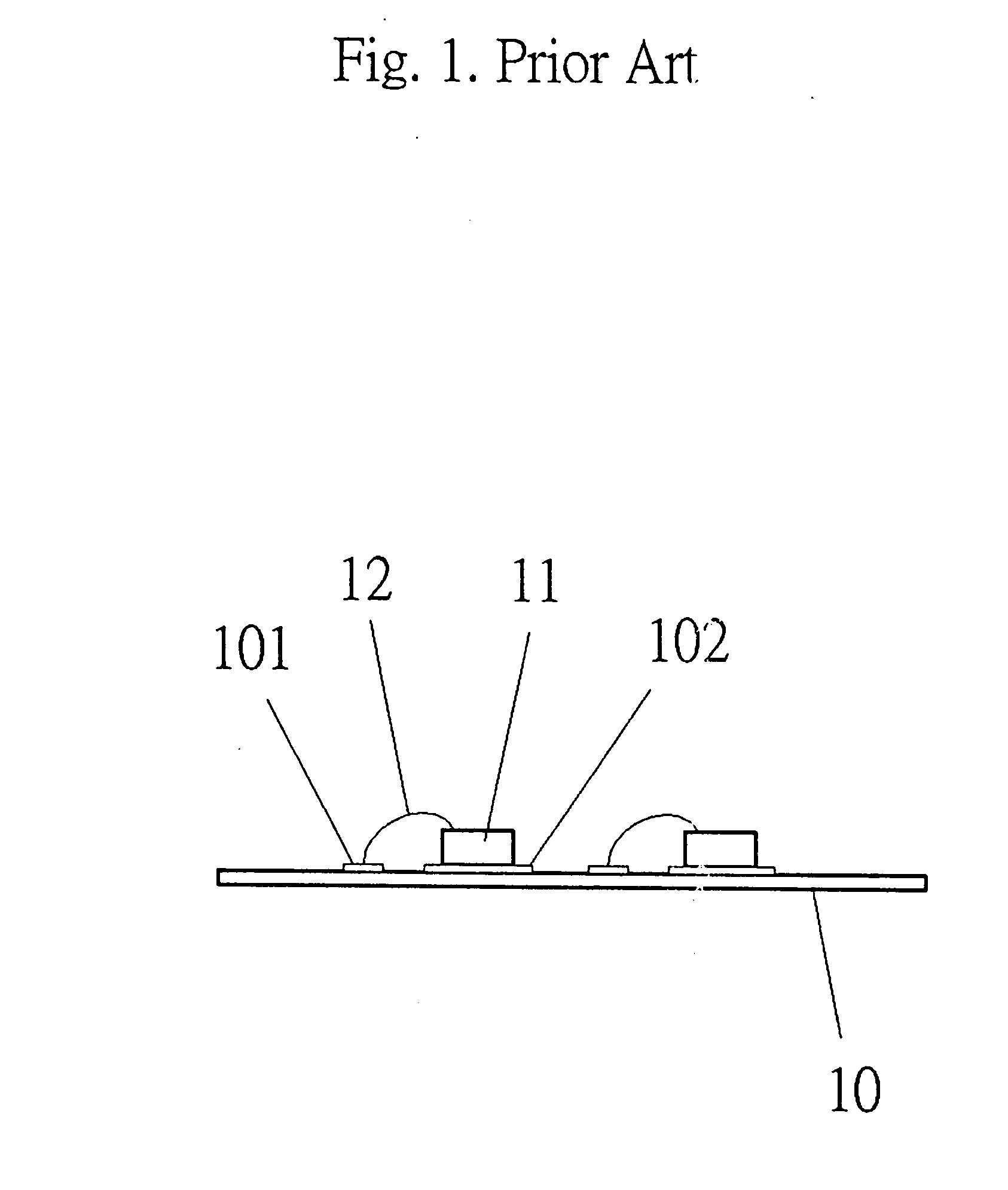
Solderless connection in LED module
a technology of led modules and soldering leads, which is applied in the direction of solid-state devices, semiconductor/solid-state device details, manufacturing tools, etc., can solve the problems of complicated process of soldering leds to printed circuits, poor heat removal, and degrading light illumination efficiency, so as to avoid complicated process and maintenance, improve the heat removal effect of light-emitting diodes, and eliminate soldering leds
- Summary
- Abstract
- Description
- Claims
- Application Information
AI Technical Summary
Benefits of technology
Problems solved by technology
Method used
Image

Examples
third embodiment
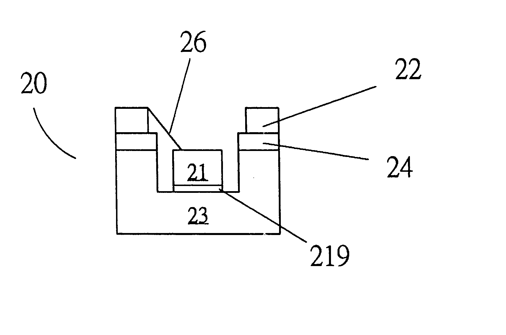
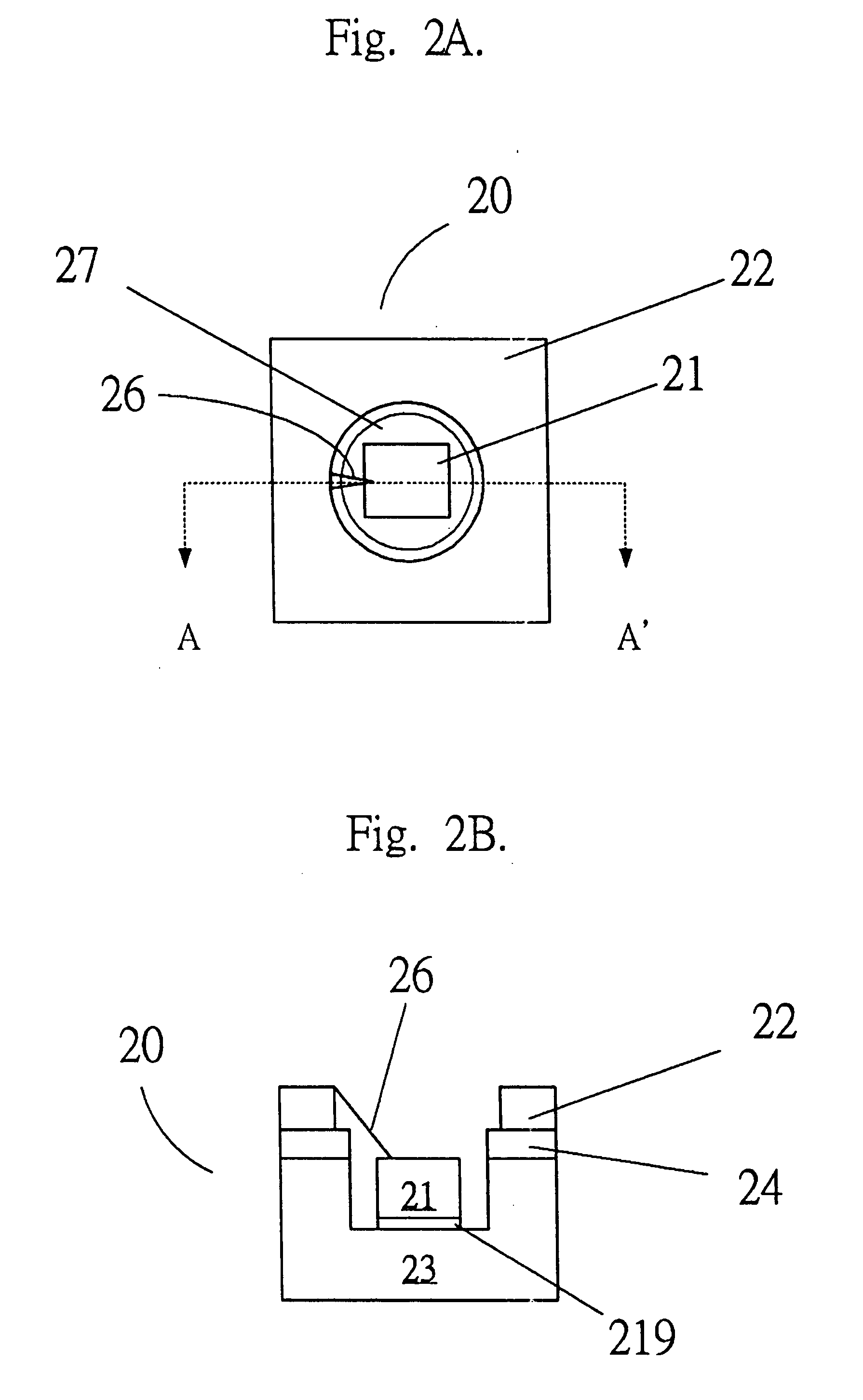
[0021]FIG. 3B shows the LED package 20. The structure is of the package 20 for LED 21 is similar to that in FIG. 3A with corresponding substrate 232 and insulating washer 24. However, the hole of the hollow upper terminal 224 is smaller that the top surface of the LED so that the inner shoulder of the upper terminal 224 lies over the rim of the LED 21, thus making contact to the top electrode of the LED 21 without using a wire.
fourth embodiment
[0022]FIG. 4A shows the LED package 20. The structure is similar to that shown in FIG. 3A with corresponding reference numerals. The only difference is that the substrate or the lower terminal 234 is recessed and the LED 21 is anchored in the recess 25.
[0023]FIG. 4B shows a fourth embodiment of the LED package 20. The structure is similar to that shown in FIG. 3B with corresponding reference numerals. The only difference is that the substrate or lower terminal 244 is recessed and the LED 21 is anchored in the recess 25.
[0024]FIG. 5 shows the basic structure of a module for housing a LED package. The module has a flat bed 29 on which the lower terminal 23 of an LED package rests, and a top pressure plate 28, which has a window 272 for the emitted light to transmit through the hole 27 of the upper terminal 22 of the LED package 20. The bed 29 is inserted with four vertical expandable telescopic posts 285 at its corners 291. The upper ends 281 of the posts are attached to four corners...
second embodiment
[0030]FIG. 9 shows the LED module for a light strip. A plurality of LED modules are lined up in a row. The top plate of the 31 is of Z-shape and is extended to become the bed of an adjacent module. In each module, the lower terminal 23 of an LED package 20 is pressed on a bed to make a solderless contact, and the upper terminal 22 is pressed to make solderless contact with the top pressure plate 31 by aligning the window 37 with the LED package 20 and sliding the holes 381 of the top plate 37 along the vertical posts 385 inserted in the holes 391 in the beds. In so doing, the LED packages in the same row are connected in series.
[0031]FIG. 10 shows a third embodiment of the LED module serving a display panel. An array of LED packages 20 are arranged in a matrix at the cross points along parallel horizontal beds 491, 492, etc. and parallel vertical top pressure bars 481, 482, etc. The bottom terminals 23 of the LED packages 20 rest on the horizontal beds, and the upper terminals 22 of...
PUM
| Property | Measurement | Unit |
|---|---|---|
| pressure | aaaaa | aaaaa |
| light transmission | aaaaa | aaaaa |
| heat removal | aaaaa | aaaaa |
Abstract
Description
Claims
Application Information