Method for producing a luminescence diode chip

Active Publication Date: 2005-07-07
OSRAM OPTO SEMICON GMBH & CO OHG
View PDF18 Cites 24 Cited by
  • Summary
  • Abstract
  • Description
  • Claims
  • Application Information

AI Technical Summary

Benefits of technology

[0022] In a further advantageous embodiment of the method, the side areas of the covering body, at least in part, are provided with a layer or layer sequence, preferably with a metallic layer, which is reflective with respect to a radia

Problems solved by technology

The separate application of the conversion layer to the covering body may be carried out under conditions which might be inherently har

Method used


Image

  • Method for producing a luminescence diode chip
  • Method for producing a luminescence diode chip
  • Method for producing a luminescence diode chip

Examples


Example

DETAILED DESCRIPTION OF THE DRAWINGS

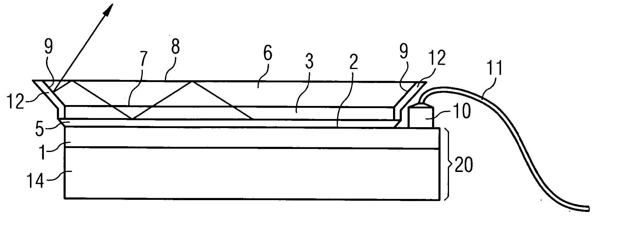
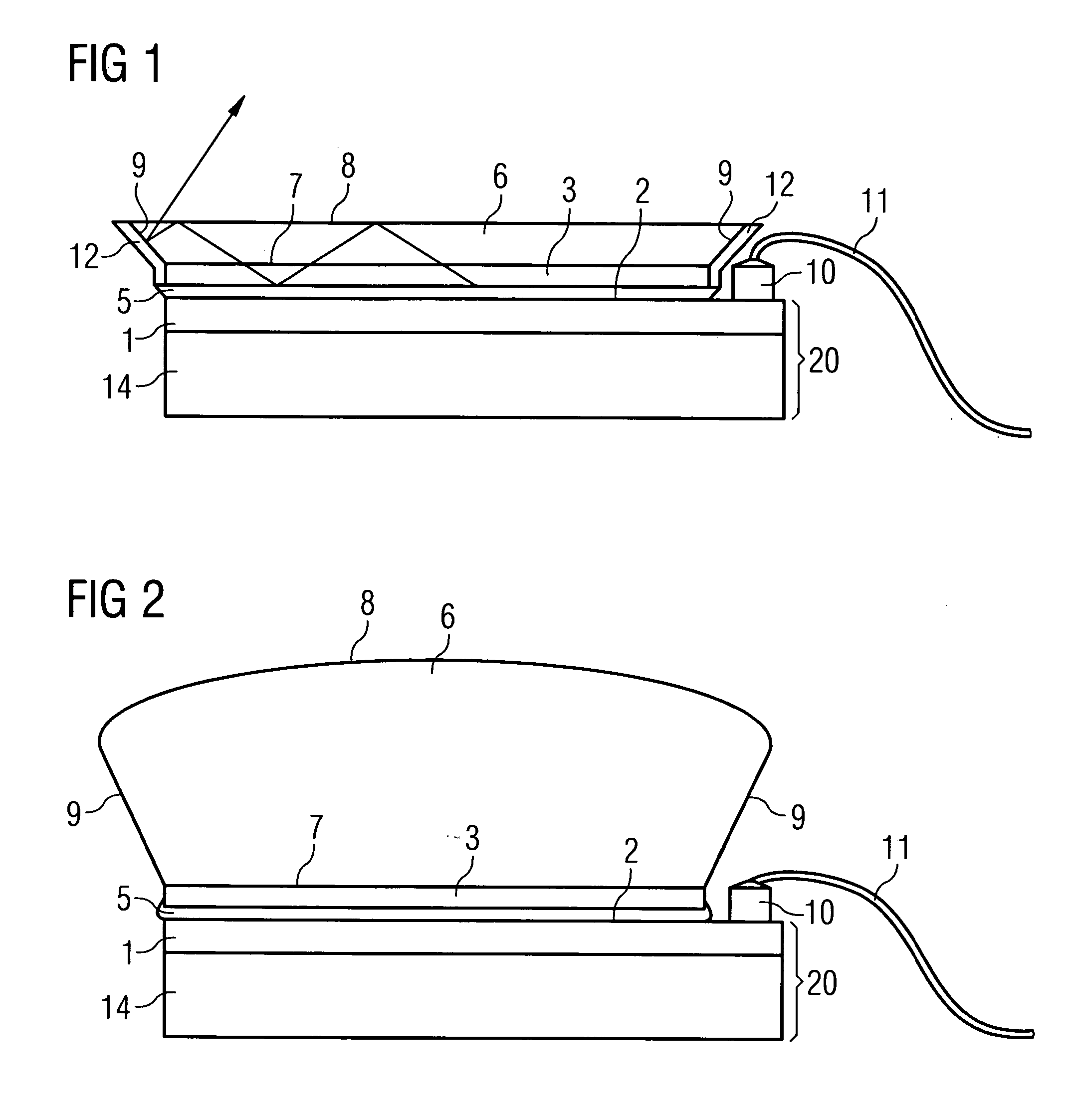
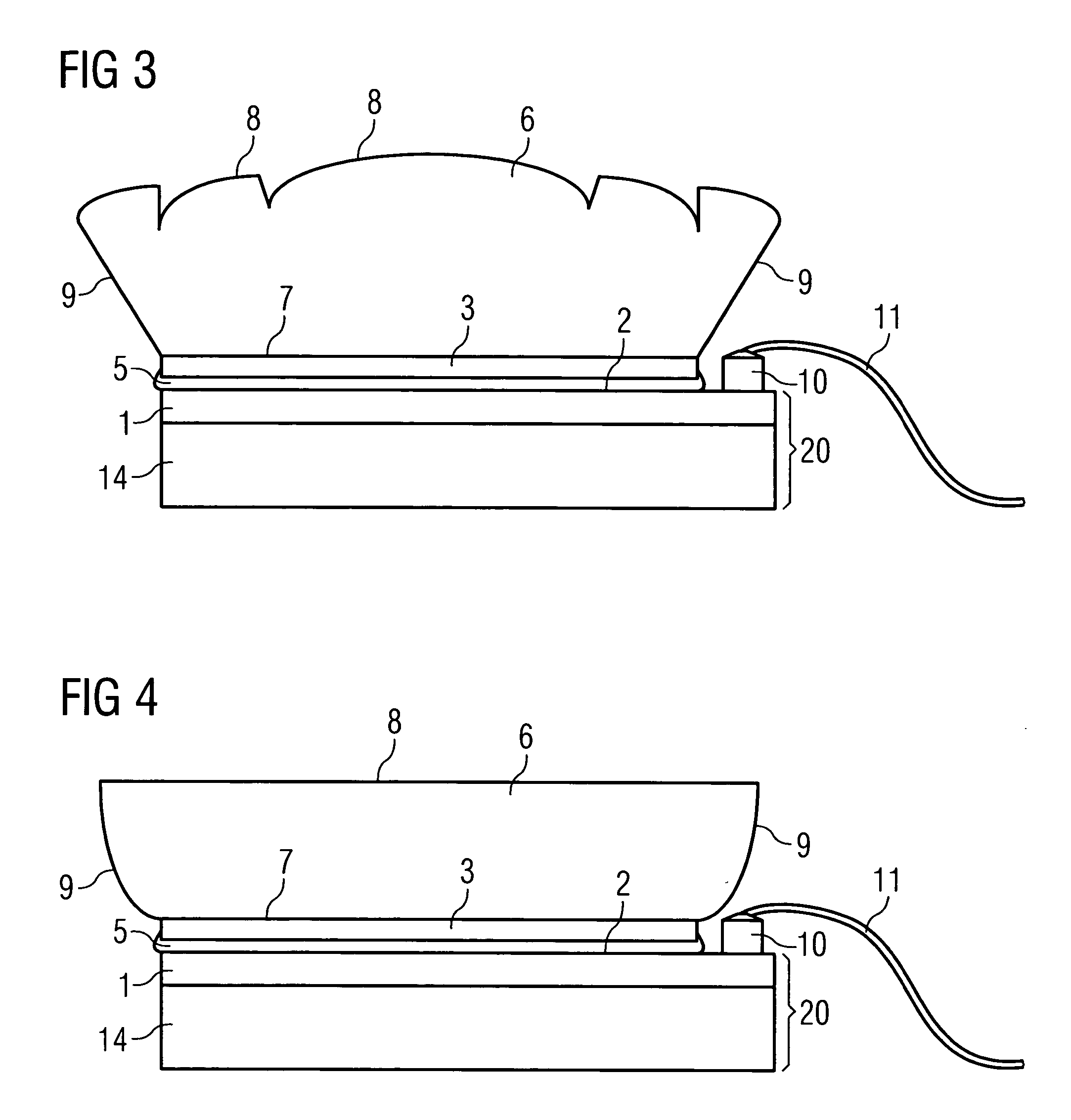
[0037] In the exemplary embodiments and figures, identical or identically active component parts are in each case provided with the same reference symbols. The component parts illustrated and also the relative sizes of the component parts among one another are not to be regarded as true to scale. Rather, some details of the figures are illustrated with their size exaggerated in order to afford a better understanding.

[0038]FIG. 1 illustrates a luminescence diode chip produced in accordance with a first exemplary embodiment of the method. This exemplary embodiment comprises the method step of providing a semiconductor body 20 having an epitaxially grown semiconductor layer sequence 1 applied on a substrate 14.

[0039] The substrate 14 may be a growth substrate, which means that the semiconductor layer sequence 1 is grown directly on the substrate 14. As an alternative, the substrate 14 may also be a carrier substrate, as is the case for example wit...


PUM


Abstract

A method for producing a luminescence diode chip, in which provision is made of a semiconductor body is provided having an epitaxially grown semiconductor layer sequence having an active zone and a radiation coupling-out area, the active zone emitting an electromagnetic radiation during operation of the luminescence diode, a large part of said electromagnetic radiation being coupled out via the radiation coupling-out area. A luminescence conversion material is arranged downstream of the radiation coupling-out area in an emission direction of the semiconductor body. A radiation-transmissive covering body having a first main area, a second main area opposite to the first main area, and also side areas connecting the first and second main areas. The covering body is applied to the radiation coupling-out area of the semiconductor layer sequence in such a way that the first main area faces the radiation coupling-out area. The application of the covering body is preceded by the application of a first conversion layer, having a luminescence conversion material, to the first main area of the covering body.

Description

RELATED APPLICATION [0001] This patent application claims the priority of German Patent Application 10351394.3, the disclosure content of which is hereby incorporated by reference. FIELD OF THE INVENTION [0002] The invention relates to a method for producing a luminescence diode chip, in which provision is made of a semiconductor body having an epitaxially grown semiconductor layer sequence having an active zone and a radiation coupling-out area, the active zone emitting an electromagnetic radiation during operation of the luminescence diode, which electromagnetic radiation, at least in part, is coupled out via the radiation coupling-out area, and in which a luminescence conversion material is arranged downstream of the radiation coupling-out area in an emission direction of the semiconductor body. BACKGROUND OF THE INVENTION [0003] A luminescence conversion material is a material having constituents by means of which an electromagnetic radiation emitted by the semiconductor layer s...

Claims


Application Information

Patent Timeline
IPC IPC(8): G21K4/00H01L21/00H01L33/50H01L33/58
CPCH01L33/58H01L33/507H01L2224/48091H01L2924/00014
Inventor OTT, HUBERTGROTSCH, STEFANBRUNNER, HERBERT
Owner OSRAM OPTO SEMICON GMBH & CO OHG
Why Eureka
Try Eureka