Semiconductor laser device

a laser device and semiconductor technology, applied in semiconductor lasers, laser optical resonator construction, laser details, etc., can solve the problems of not yielding actually satisfactory beam quality or and the output power of the semiconductor laser device is comparatively low, so as to achieve the effect of relatively easy operation

Inactive Publication Date: 2006-07-27
LIMO PATENTVERWALTUNG GMBH & CO KG
View PDF8 Cites 32 Cited by
  • Summary
  • Abstract
  • Description
  • Claims
  • Application Information

AI Technical Summary

Benefits of technology

[0013] As described in the invention, it is furthermore possible for the semiconductor laser element to be exposed to a voltage and to be supplied with current for producing electron-hole pairs only in partial areas which c

Problems solved by technology

The disadvantage in this semiconductor laser device is that on the one hand due to the many optical components within the external resonator comparatively high losses occur so that the output power of the semiconductor laser device is comparatively

Method used


Image

  • Semiconductor laser device
  • Semiconductor laser device
  • Semiconductor laser device

Examples


Embodiment Construction

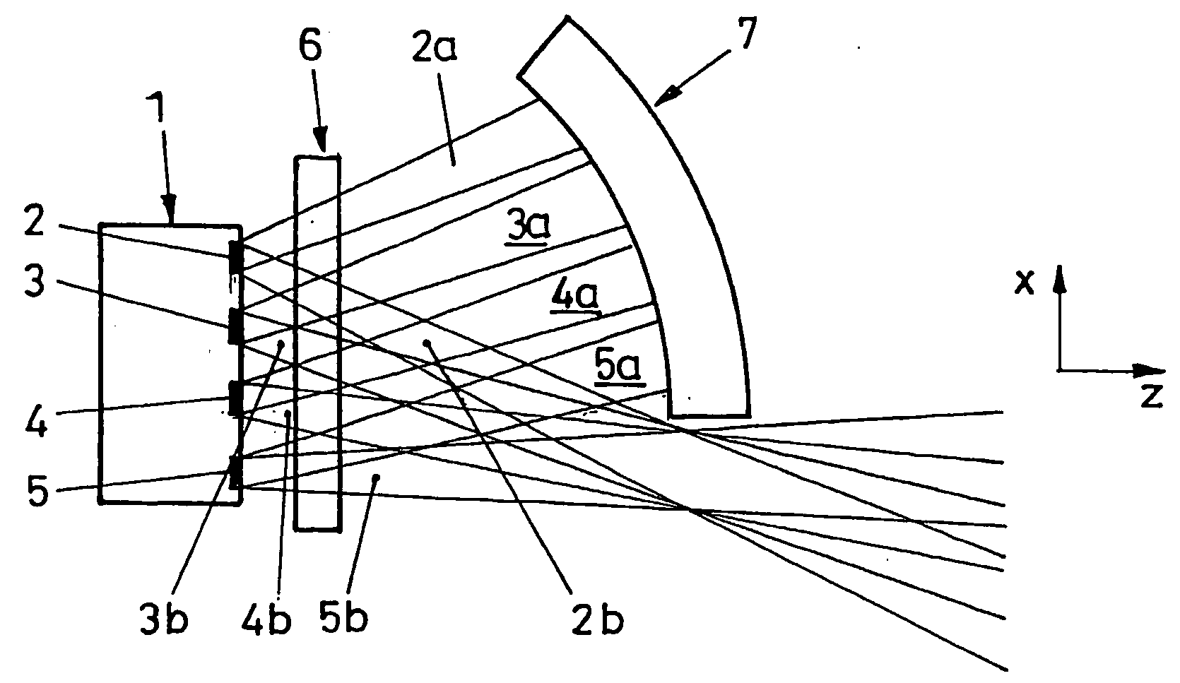
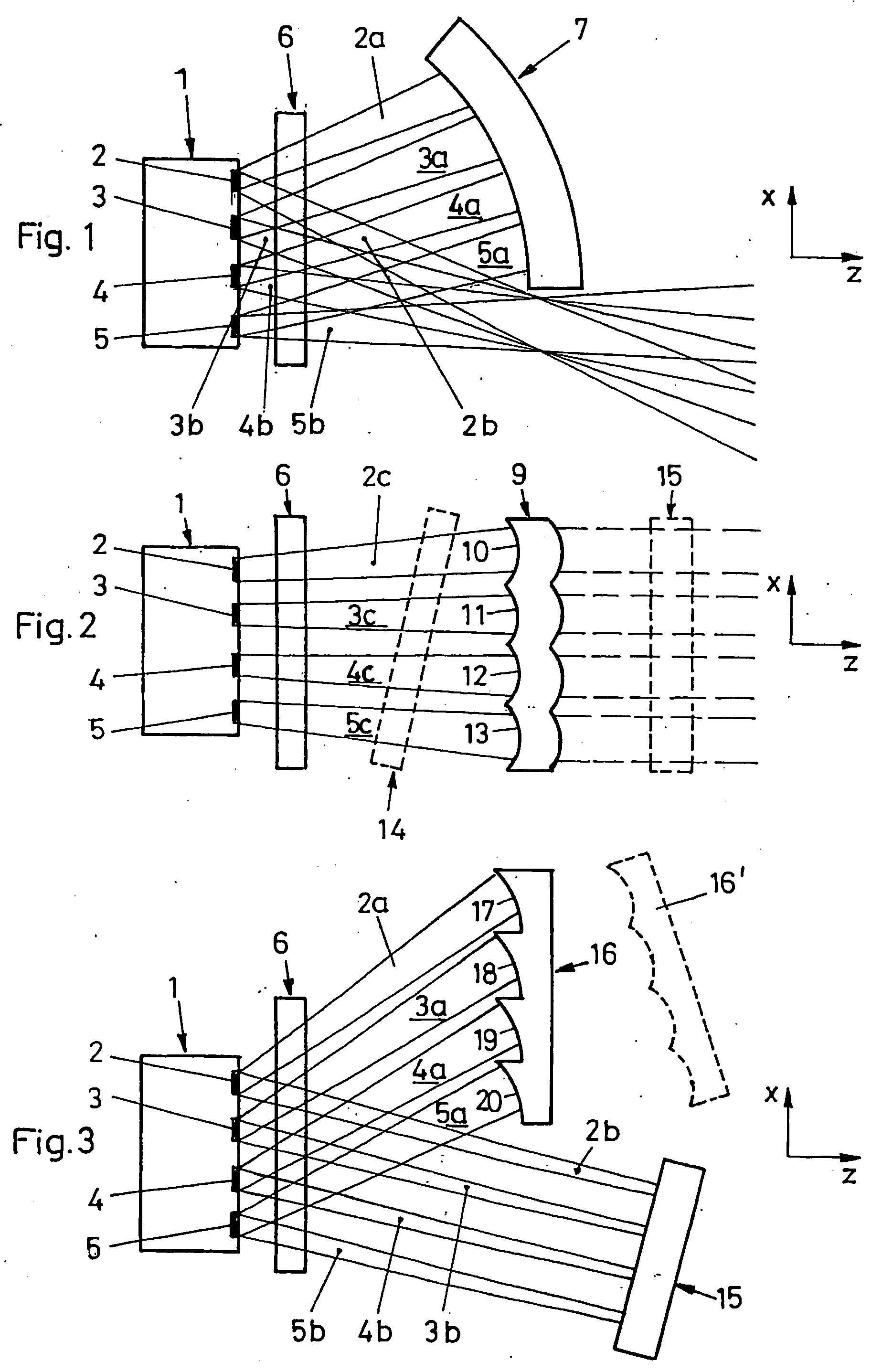
[0019] The embodiment of a semiconductor laser device as described in the invention shown in FIG. 1 includes a semiconductor laser element 1 with a host of exit surfaces 2, 3, 4, 5 from which laser light can emerge. The semiconductor laser element 1 is made as a broad strip emitter array or as a so-called laser diode bar. In the illustrated embodiment, only four exit surfaces 2, 3, 4, 5 which are separated from one another and which are used for light emission are shown. But it is quite possible for there to be a much larger number of exit surfaces which are arranged parallel and spaced apart from one another.

[0020] The laser light emerging from each of the exit surfaces 2, 3, 4, 5 is split into two component beams 2a, 2b; 3a, 3b; 4a, 4b; 5a, 5b which each include an oppositely identical angle with the normals to the exit surfaces 2, 3, 4, 5. The paired component beams 2a, 2b; 3a, 3b; 4a, 4b; 5a, 5b each represent a selected laser mode of the emitting component area of the semicond...


PUM


Abstract

The invention relates to a semiconductor laser devcie, including a semiconductor laser element, or a number of individual lasers mounted parallel to each other, with a number of output surfaces, from which laser light can escape, having a treater divergence in a first direction (Y) than in a second direction parallel to the above and at least one reflecting means, at a distance from the output surfaces, outside the semiconductor laser element or the individual laser, with at least one reflective surface which reflects at least a part of the laser light escaping from the semiconductor laser element or the individual lasers through the output surfaces back into the semiconductor laser element or the individual lasers, such that the mode spectrum of the semiconductor laser element or the individual lasers is influenced. The at least one reflective surface of the reflecting means has a concave curve.

Description

BACKGROUND OF THE INVENTION [0001] This invention relates to a semiconductor laser device including a semiconductor laser element or a plurality of individual lasers mounted in parallel with a plurality of exit surfaces from which laser light can emerge, which in a first direction has greater divergence than in the second direction which is perpendicular to it, and at least one reflection means which is located spaced apart from the exit surfaces outside of the semiconductor laser element or the individual lasers, with at least one reflecting surface which can reflect back at least parts of the light which has emerged from the semiconductor laser element or the individual lasers through the exit surfaces into the semiconductor laser element or the individual lasers such that the mode spectrum of the semiconductor laser element or of the individual lasers is influenced thereby. [0002] A semiconductor laser device of the aforementioned type is known from I. Nelson, B. Chann, T. G. Wal...

Claims


Application Information

Patent Timeline
IPC IPC(8): H01S5/00H01S5/14H01SH01S5/065H01S5/40
CPCH01S5/0267H01S5/0656H01S5/4012H01S5/4031H01S5/4062H01S5/065H01S5/14
Inventor MIKHAILOV, ALEKSEIHARTEN, PAUL ALEXANDERHILL, WIELAND
Owner LIMO PATENTVERWALTUNG GMBH & CO KG
Why Eureka
Try Eureka