Method for fabricating a flash-preventing window ball grid array semiconductor package

a technology of semiconductor packages and window balls, applied in the field of semiconductor package fabrication methods, can solve the problems of undesirable yield issues of wbga packages, adversely affecting the quality of electrical connections of semiconductor packages, damage to surface planarity and external appearance, etc., and achieve the effect of reducing flow speed and increasing viscosity

Inactive Publication Date: 2005-07-07
HUANG CHIEN PING
View PDF13 Cites 2 Cited by
  • Summary
  • Abstract
  • Description
  • Claims
  • Application Information

AI Technical Summary

Benefits of technology

[0006] An objective of the present invention is to provide a flash-preventing window ball grid array (WBGA) semiconductor package, a method for fabricating the semiconductor package, and a chip carrier used in the semiconductor package, which can assure the quality of electrical connection.
[0007] Another objective of the present invention is to provide a flash-preventing WBGA semiconductor package, a method for fabricating the semiconductor package, and a chip carrier used in the semiconductor package, which can improve the surface planarity of the semiconductor package.
[0008] A further objective of the present invention is to provide a flash-preventing WBGA semiconductor package, a method for fabricating the semiconductor package, and a chip carrier used in the semiconductor package, which can provide a clean and satisfactory appearance for the semiconductor package.
[0013] Therefore, during the molding process, the encapsulating material forming the second encapsulation body encapsulates the bonding wires and is filled in the narrow runner, such that the second encapsulation body covering the intended-exposing regions has a substantially equal thickness to that of the solder mask layer. As the encapsulating material is a viscous fluid having a low Reynolds number, when it enters into the constricted narrow runner, according to the fluid mechanics, the encapsulating material or viscous fluid would have its viscosity increased and its flow speed reduced, such that the encapsulating material stops its motion within the narrow runner without flashing into an interface between the solder mask layer and the surface of the mold or over the ball-bonding portions, thereby eliminating the occurrence of resin flash and assuring the quality of electrical connection of the semiconductor package.

Problems solved by technology

Besides the above mentioned benefits, however, the WBGA package undesirably renders a yield issue.
This resin flash f not only damages the surface planarity and external appearance of the semiconductor package, but also possibly contaminates the ball-bonding regions 85 predefined on the second surface 82 of the substrate 80, making the solder balls 92 fail to be perfectly bonded to the substrate 80 and thus adversely affecting the quality of electrical connection of the semiconductor package.

Method used


Image

  • Method for fabricating a flash-preventing window ball grid array semiconductor package
  • Method for fabricating a flash-preventing window ball grid array semiconductor package
  • Method for fabricating a flash-preventing window ball grid array semiconductor package

Examples


Embodiment Construction

[0024] The preferred embodiments of a flash-preventing window ball grid array (WBGA) semiconductor package and a method for fabricating the semiconductor package proposed in the present invention are described with reference to FIGS. 1, 2A-2B, 3, and 4A-4F.

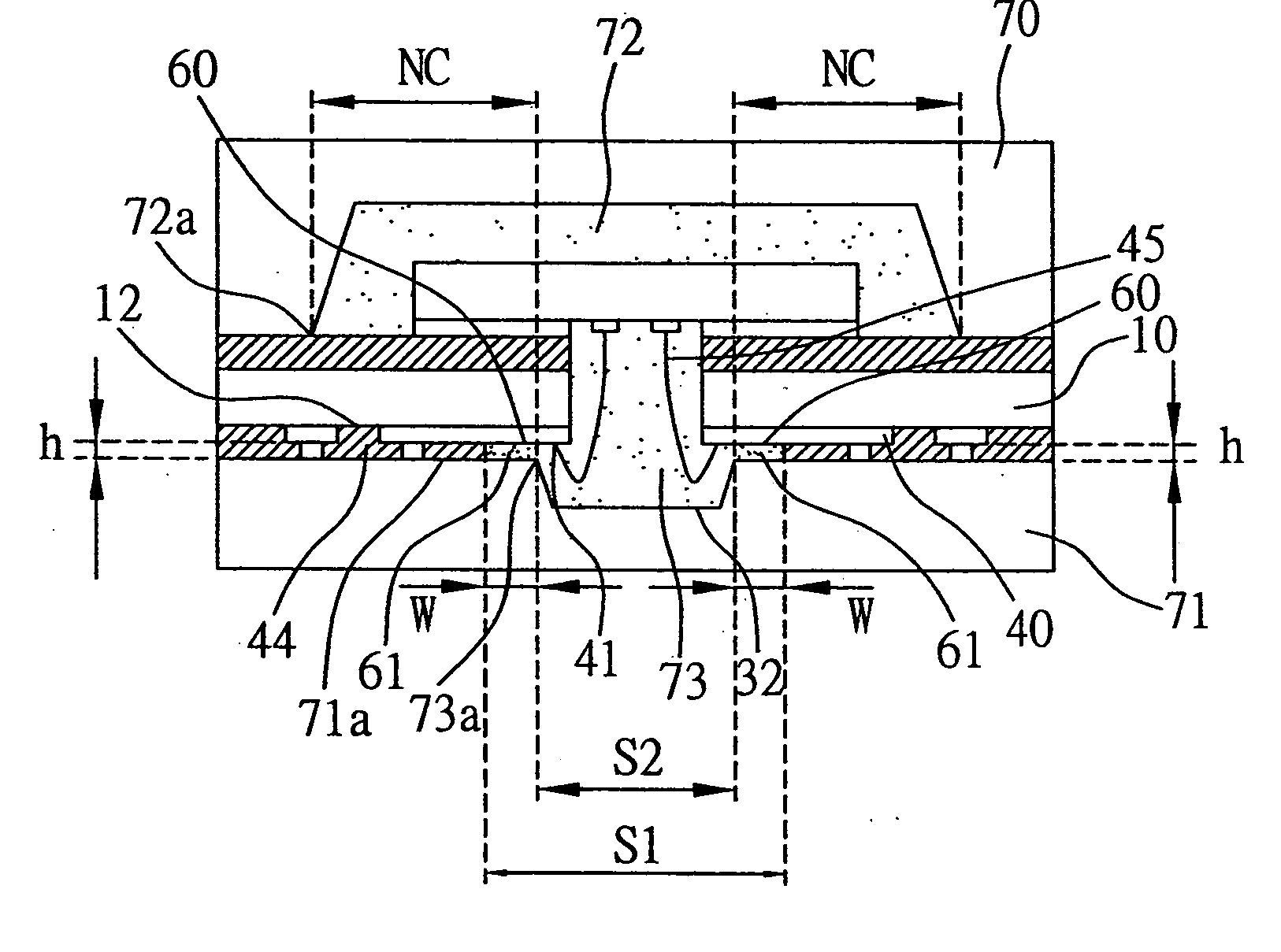
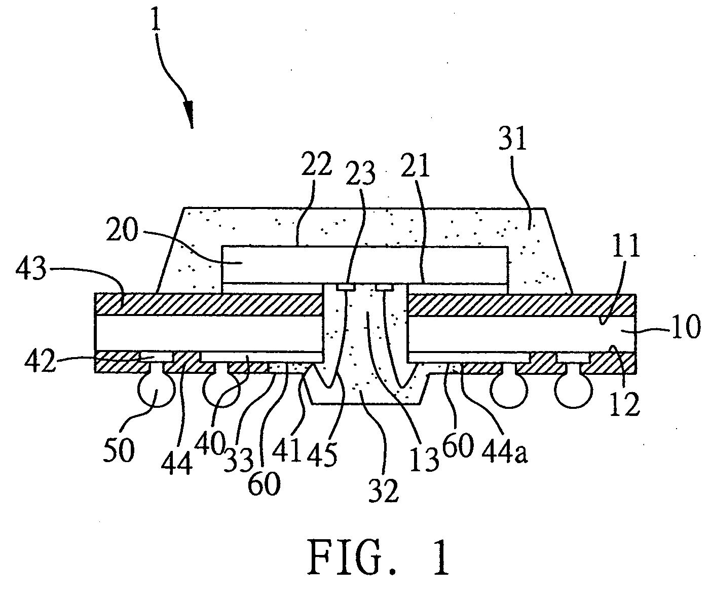
[0025]FIG. 1 shows a cross-sectional view of the WBGA semiconductor package 1 according to a preferred embodiment of the invention, comprising: a substrate or core layer 10 having a first surface 11 and an opposite second surface 12; a chip 20 mounted on the substrate 10 and having an active surface 21 and an inactive surface 22; first and second encapsulation bodies 31, 32 formed on the first surface 11 and the second surface 12 of the substrate 10 respectively; and a plurality of solder balls 50 deposited on the second surface 12 of the substrate 10. In more detail, a through hole 13 is formed at the center of the substrate 10 and penetrates through the substrate 10. A plurality of conductive traces 40 are formed on the second ...


PUM


Abstract

A flash-preventing window ball grid array semiconductor package, a method for fabricating the same, and a chip carrier used in the semiconductor package are provided. The chip carrier has a through hole and has a surface formed with a plurality of wire-bonding portions, ball-bonding portions and intended-exposing regions. A chip is mounted over the through hole and electrically connected to the wire-bonding portions by a plurality of bonding wires penetrating through the through hole. An encapsulation body encapsulates the chip and bonding wires. The intended-exposing regions serve as a narrow runner which is filled with an encapsulating material forming the encapsulation body, making the encapsulating material not flash over the ball-bonding portions. This allows a plurality of solder balls to be well bonded to the ball-bonding portions, thereby assuring the quality of electrical connection and the surface planarity of the semiconductor package.

Description

FIELD OF THE INVENTION [0001] The present invention relates to semiconductor packages and fabrication methods thereof, and more particularly, to a window ball grid array (WBGA) semiconductor package which can prevent the occurrence of resin flash and assure the quality of electrical connection, and a method for fabricating the semiconductor package, as well as a chip carrier used in the semiconductor package. BACKGROUND OF THE INVENTION [0002] A conventional window ball grid array (WBGA) semiconductor package uses a substrate having at least one through hole penetrating therethrough to allow a chip to be mounted on a surface of the substrate and over the through hole. A plurality of bonding wires go through the through hole and electrically connect the chip to the substrate. A plurality of solder balls are formed on a surface opposite to the chip-mounting surface of the substrate to electrically connect the chip to an external electronic device. This WBGA structure desirably shorten...

Claims


Application Information

Patent Timeline
Patent Type & Authority Applications(United States)
IPC IPC(8): H01L21/56H01L21/82H01L23/13H01L23/31H01L23/48H01L23/495H01L23/498H01L23/52H01L27/10H01L29/40H01L29/739H01L31/0203
CPCH01L21/565H01L23/13H01L24/49H01L24/48H04N5/2257H01L2924/15311H01L23/3114H01L23/3128H01L23/49572H01L23/49816H01L31/0203H01L2224/48091H01L2224/4824H01L2224/49175H01L2924/00014H01L2924/00H04N23/57
Inventor HUANG, CHIEN-PING
Owner HUANG CHIEN PING
Why Eureka
Try Eureka