Sensors

a technology of sensors and sensors, applied in the field of sensors, can solve problems such as adding to manufacturing costs

Active Publication Date: 2005-07-14
STMICROELECTRONICS (RES & DEV) LTD
View PDF0 Cites 5 Cited by
  • Summary
  • Abstract
  • Description
  • Claims
  • Application Information

AI Technical Summary

Benefits of technology

[0005] In view of the foregoing background, an object of the invention is to provide a method for forming 3D structures reliably and inexpensively on the surface of a sensor. The method may be easily incorporated into existing manufacturing processes.

Problems solved by technology

However, these methods currently require special technology, processing and equipment which add to the manufacturing cost.

Method used


Image

  • Sensors
  • Sensors
  • Sensors

Examples


first embodiment

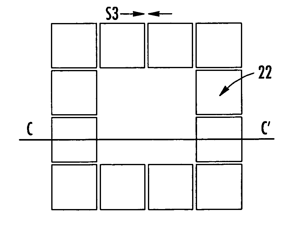
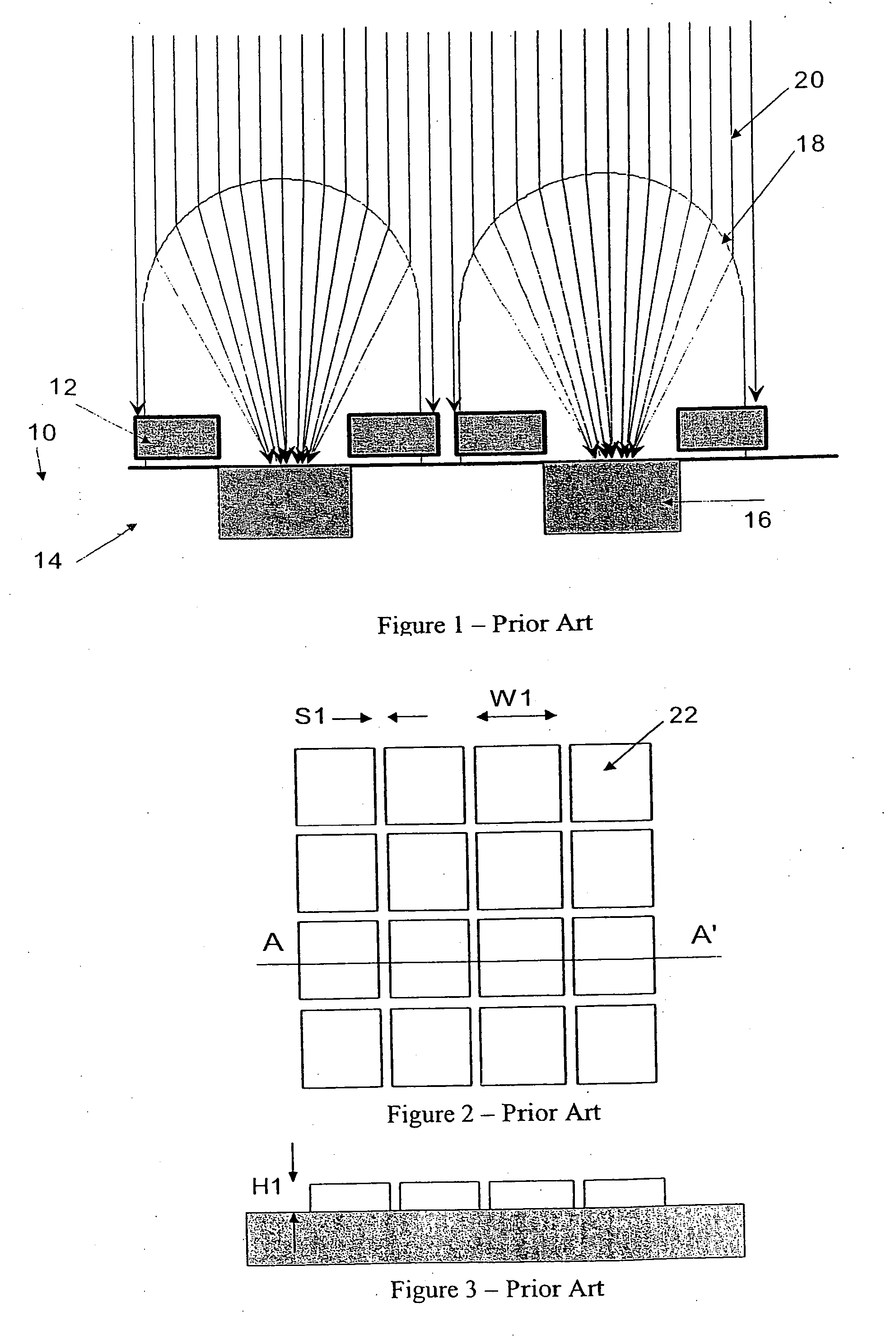
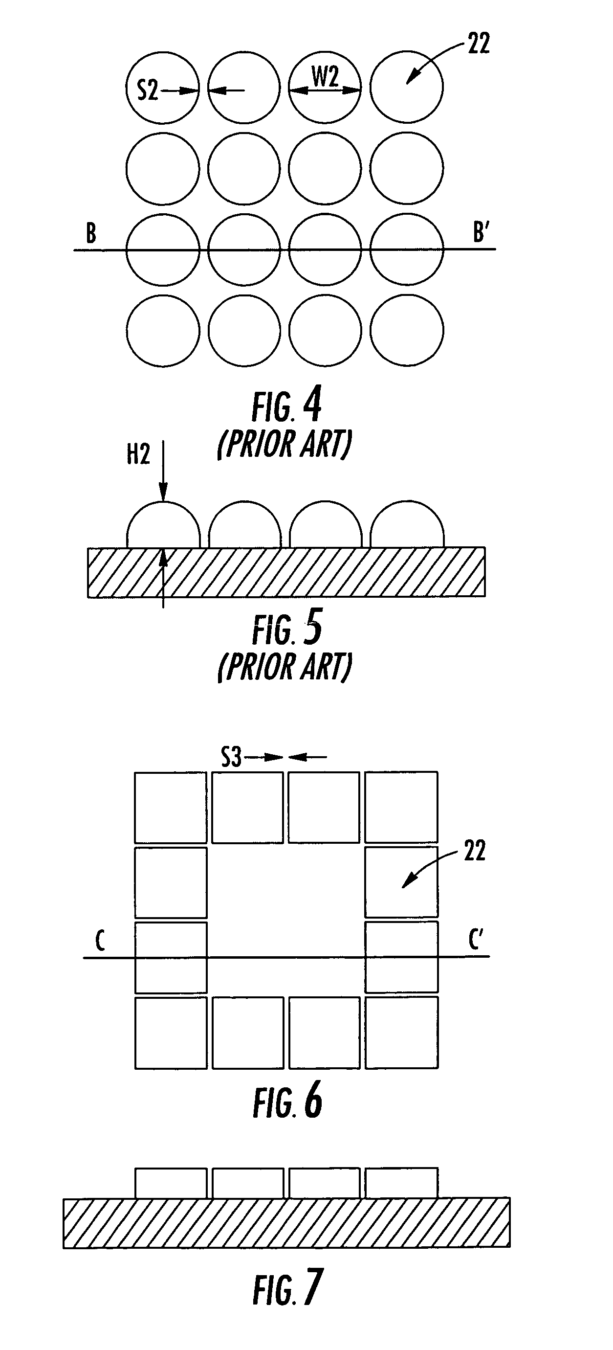
[0027]FIGS. 6-9 illustrate the present invention. As shown in FIG. 6, photoresist volume portions 22 are spaced apart by a distance S3, where S31, and are formed in a defined shape, namely a ring. The value of S3 is chosen to ensure that adjacent volume portions 22 merge together during reflow. S3 could even be made as low as zero.

[0028] When S3 is zero, a reflow step is not necessary to ensure that a barrier of photoresist material is formed for defining a region suitable for constraining bio-optical reagent or analyte sample materials. However, a reflow step can still be performed to ensure that the edges and walls of the patterned regions and channels are smoother. The increased smoothness helps to reduce resistance to the flow of bio-optical reagent or analyte sample materials.

[0029] During the heating process the microlens material will melt. As the squares are closed, under the influence of gravity, the material will touch and surface tension will cause them to join up. FIG. ...

fourth embodiment

[0032] More complex shapes can also be constructed. FIG. 14 shows a fourth embodiment, where four annuli as shown in FIG. 6 are combined to form a microlens structure 32 comprising four sites 34.

[0033] With this structure, four different reagents could be deposited at each of the four sites 34. The microlens material 32 provides an effective barrier between the sites to isolate reagents located in the neighboring sites 34. This sensor could then provide the sensing and / or detection of up to four different chemicals in the analyte.

fifth embodiment

[0034]FIG. 15 shows a fifth embodiment, where two sites 36, 40 are connected by a channel 38. The connection allows the analyte to flow between different sites.

[0035] It will be appreciated that the regions formed by the particular shapes and formations referred to above are only a very few of a large number of regions that can be formed using the techniques of the present invention, and the present invention is in no way to be considered as being limited to these particular regions.

[0036] The principles of the invention, when applied to bio-optical sensor systems, allow both accurate deposition of a reagent during manufacture of the system and also the production of channels and guides to assist the flow of the analyte during operation of the system.

[0037] It is also to be recognized that the top surface of the sensor is usually formed from silicon nitride to protect the device. This material can also be patterned and etched to provide similarly defined regions that serve similar...


PUM

PropertyMeasurementUnit
distanceaaaaaaaaaa
temperatureaaaaaaaaaa
volumesaaaaaaaaaa

Abstract

A method for forming a sensor is provided, together with a sensor formed according to the method. Photoresist material is deposited on a surface of the sensor, and is then patterned and etched to form an array of microlens structures. The structures are spaced close together in a predetermined pattern so that when a reflow process is performed, the structures melt and coalesce to form a barrier. The barrier defines a region for constraining or channeling the flow of reagent and analyte samples used in bio-optical sensors.

Description

FIELD OF THE INVENTION [0001] The present invention relates to sensors, and in particular, to a method of forming a sensor and a sensor produced in accordance with that method. BACKGROUND OF THE INVENTION [0002] Bio-optical sensors detect photo-emissive chemical reactions between an analyte and a reagent. Improved bio-optical sensors have a number of different reagents to enable them to detect the presence / concentration of several analytes. During the manufacture of such sensors, it is necessary to locate and separate the reagents, and during their operation, it is necessary to guide the sample containing the analyte over the sensor sites. [0003] The sites should be mechanically isolated. Suitable structures may be patterned and etch, either on the silicon of the sensor surface or by making trenches in the silicon itself. However, these methods currently require special technology, processing and equipment which add to the manufacturing cost. [0004] When forming a structure on the s...

Claims


Application Information

Patent Timeline
Patent Type & Authority Applications(United States)
IPC IPC(8): B01L3/00G01N33/543G02B3/00G03F7/40
CPCB01L3/5085B01L2200/12B01L2300/0819G03F7/40G02B3/0018G02B3/0056G01N33/543
Inventor RAYNOR, JEFFREY
Owner STMICROELECTRONICS (RES & DEV) LTD
Why Eureka
Try Eureka