Mounting substrate and electronic component using the same

Inactive Publication Date: 2005-07-14
TDK CORPARATION
View PDF9 Cites 3 Cited by
  • Summary
  • Abstract
  • Description
  • Claims
  • Application Information

AI Technical Summary

Benefits of technology

[0012] Therefore, an object of the present invention is to provide a mounting substrate which can reduce the mounting area when being mounted on an external connection substrate, and an electronic component using this mounting substrate.
[0013] Further, an object of the present invention is to provide a mounting substrate capable of reducing characteristic deterioration caused by generation of parasitic components, and an electronic component using this mounting substrate.
[0014] Furthermore, an object of the present invention is to provide a mounting substrate capable of achieving uniformity of the area of the external connection terminal between the mounting substrates, and an electronic component using this mounting substrate.

Problems solved by technology

Therefore, especially in the case where the electronic device 20 is a high frequency device, the characteristics thereof may be deteriorated.
Therefore, in order to avoid such a defect, it is necessary to have a complex pattern configuration in which the pattern is rotated 180 degrees around for each line, which provides no freedom of pattern formation.

Method used


Image

  • Mounting substrate and electronic component using the same
  • Mounting substrate and electronic component using the same
  • Mounting substrate and electronic component using the same

Examples


Embodiment Construction

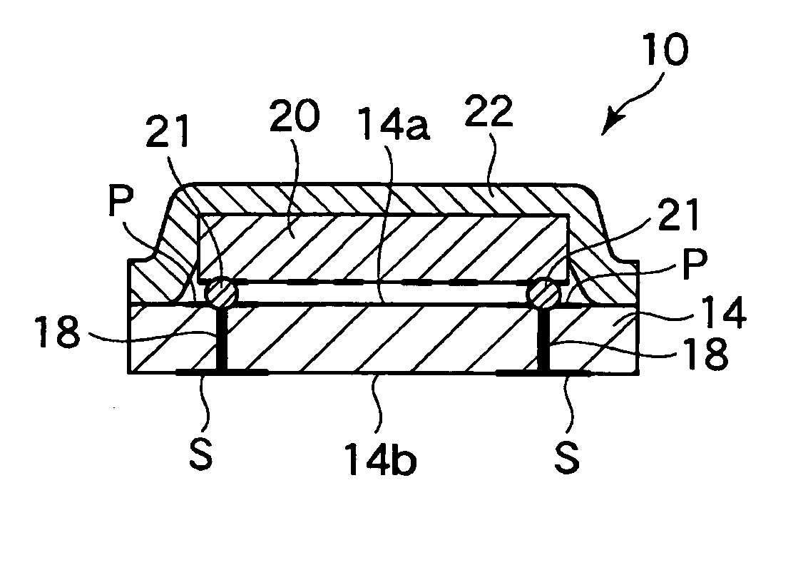
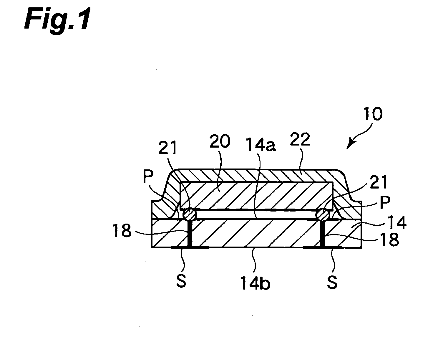
[0036] The best mode for carrying out the present invention will now be described in more detail hereinbelow with reference to the drawings. The same members will be denoted by the same reference symbols throughout the accompanying drawings, without redundant description. It is noted that the description herein concerns the best mode for carrying out the present invention and that the present invention is by no means intended to be limited to the mode.

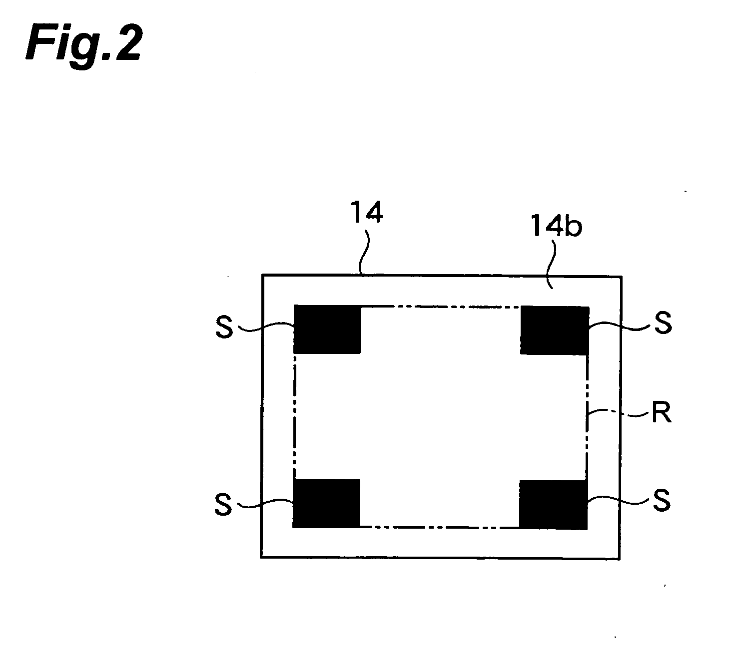
[0037]FIG. 1 is a cross sectional view showing an electronic component of an embodiment of the present invention, FIG. 2 is a bottom view showing a mounting substrate constituting the electronic component of FIG. 1, FIG. 3 is a cross sectional view showing a state in which the electronic component of FIG. 1 is mounted on an external connection substrate, FIG. 4 is an explanatory drawing showing a mounting substrate which is a separated individual piece constituting the electronic component of FIG. 1, and a collective substrate prior t...


PUM


Abstract

A mounting substrate of an embodiment of the present invention comprises a first main surface constituting a mounting surface on which an electric device is mounted, and having formed thereon an electrode pattern comprising a plurality of electrode pads that are electrically connected to the electronic device via a bump, and a second main surface which is positioned on the opposite side of the first main surface, and which has formed thereon a plurality of input / output terminals that are electrically connected to the electrode pads. All of the input / output terminals are formed in positions apart from the periphery of the mounting substrate.

Description

BACKGROUND OF THE INVENTION [0001] 1. Field of the Invention [0002] The present invention relates to a mounting substrate, and to an electronic component using the same. [0003] 2. Related Background of the Invention [0004] Today, miniaturization of the mobile communication apparatus typified by the remarkably spreading cellular phones has been developing progressively. With this miniaturization, further miniaturization of the electronic components used in the mobile communication apparatus has been demanded. [0005] For this reason, in a conventional electronic component 100, as shown in FIG. 6, an electronic device 20 in which a circuit element is formed on a device substrate is mounted on a mounting substrate 14 in a face-down manner through a bump 21. The electronic component 100 is constituted by sealing this electronic device 20 by mean of a sealing portion 22, such as a cap or resin. [0006] In the prior art, an electrode 30 is disposed on a side surface of the mounting substrat...

Claims


Application Information

Patent Timeline
IPC IPC(8): H01L21/60H01L23/12H01L23/31H01L23/48H01L23/498H03H9/02H03H9/10H03H9/17H03H9/25
CPCH01L23/3121H01L2224/16235H01L23/49838H01L24/97H01L2224/16H01L2224/97H01L2924/01015H01L2924/01033H01L2924/01078H01L2924/01082H01L2924/19041H01L2924/19042H01L2924/19043H01L2924/30105H01L2924/30107H01L2924/3025H03H9/059H03H9/1085H01L23/49805H01L2924/01006H01L2924/01005H01L2224/81
Inventor ADACHI, TAKUYAINOUE, KENJI
Owner TDK CORPARATION
Why Eureka
Try Eureka