Electronic device, electronic apparatus, moving object, and method for manufacturing electronic device

a technology of electronic devices and moving objects, which is applied in the direction of semiconductor devices, solid-state devices, printed electric components, etc., can solve the problems of difficult downsizing and thinning of electronic devices, and achieve the effect of high heat conductivity, efficient conductivity and high heat conductivity

Active Publication Date: 2014-10-02
SEIKO EPSON CORP
View PDF0 Cites 3 Cited by
  • Summary
  • Abstract
  • Description
  • Claims
  • Application Information

AI Technical Summary

Benefits of technology

[0051]The heating element 42 such as, for example, a power transistor or a heater is connected to the resonator 40 by means of a bonding member 56 having a high heat conductivity such as solder on the mounting terminal 26 disposed on the one main surface of the resonator 40. By connecting the heating element 42 using the bonding member 56 having a high heat conductivity, the heat from the heating element 42 is efficiently conducted to the resonator 40, and the power consumed by the heating element 42 is reduced. Therefore, there is an advantageous effect that the electronic device 1 with low power consumption is obtained. The mounting terminal 26 is electrically connected to a ground terminal (not shown) of the electronic device 1 through the lead frame terminal 30 with an electrode wiring (not shown) disposed on the one main surface of the resonator 40, so that the occurrence of an electrical noise is prevented.
[0052]The thermosensor 44 such as, for example, a thermistor or a quartz crystal resonator for temperature sensor is electrically connected to the resonator 40 by means of a conductive bonding member 58 such as a solder or metal bump on the mounting terminal 28 disposed on the one main surface of the resonator 40. The thermosensor 44 is electrically connected to the IC chip 46 including the temperature control circuit through the lead frame terminal 30 with an electrode wiring (not shown) disposed on the one main surface of the resonator 40.
[0053]The lead frame terminal 30 as a support member includes the first terminal 34 and a second terminal 36 at both ends of a support portion 32. Two notch portions 38 are arranged in the first terminal 34 such that the notch portions 38 are spaced apart from each other with a gap corresponding to the width of the support portion 32 on the side where the first terminal 34 is coupled with the support portion 32. Since the notch portions 38 are disposed in the first terminal 34, the first terminal 34 can be bent at the central portion thereof or at a position close to the inner side of the outer edge of the resonator 40, which is advantageous for a reduction in mounting area to the board 10. The width of the support portion 32 is smaller than the width of the first terminal 34. The reason of this is to reduce the conduction of heat of the heating element 42 to the board 10 through the support portion 32 while maintaining the bonding strength at the first terminal 34. The first terminal 34 of the lead frame terminal 30 is connected with the third terminal 20 of the resonator 40. The second terminal 36 is connected by means of a conductive third bonding member 54 to a lead electrode 16 disposed on the board 10, and therefore electrically connected to the lead electrode 16.
[0054]As shown in FIG. 13, the first terminal 34 of the lead frame terminal 30 is bent toward the board 10 side in the vicinity where the notch portions 38 are disposed (refer to FIG. 2). Further, the support portion 32 is bent such that the second terminal 36 is substantially parallel to the board 10. Therefore, the first terminal 34 and the second terminal 36 are substantially parallel to the main surface of the resonator 40 or the board 10. Hence, by connecting the second terminals 36 to the plurality of lead electrodes 16 disposed on the board 10, the resonator 40 to which the heating element 42 and the thermosensor 44 are connected can be supported in a state of floating above the board 10. Therefore, the heat from the heating element 42 that heats the resonator 40 is less likely to be conducted to the board 10 through the lead frame terminal 30 as a support member, so that there is an advantageous effect that low power consumption of the electronic device 1 can be achieved.
[0055]The IC chip 46 including the oscillator circuit for driving the resonator 40 and the temperature control circuit that controls the heating element 42 based on temperature information from the thermosensor 44 is connected by means of conductive bonding members 38 to mounting electrodes 18 disposed on the board 10, and therefore electrically connected to the mounting electrodes 18. Since the electronic device 1 has a structure in which the resonator 40 is supported in a state of floating above the board 10, the IC chip 46 can be mounted in a space between the resonator 40 and the board 10. Therefore, the board 10 can be made small, so that the downsizing of the electronic device 1 can be achieved.
[0056]Next, the shape of the lead frame terminal 30, which enables the downsizing of the electronic device 1, will be described.

Problems solved by technology

Therefore, there is a problem that it is very difficult to achieve the downsizing and thinning of the electronic device.
Therefore, there is a problem that the downsizing is difficult.

Method used


Image

  • Electronic device, electronic apparatus, moving object, and method for manufacturing electronic device
  • Electronic device, electronic apparatus, moving object, and method for manufacturing electronic device
  • Electronic device, electronic apparatus, moving object, and method for manufacturing electronic device

Examples


modified example 1

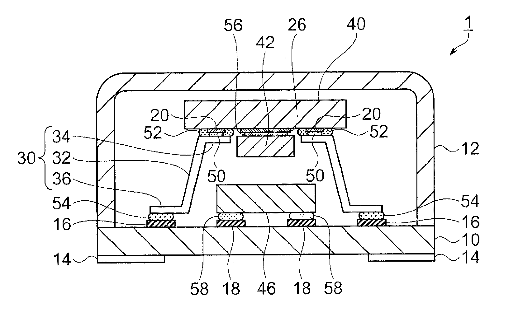
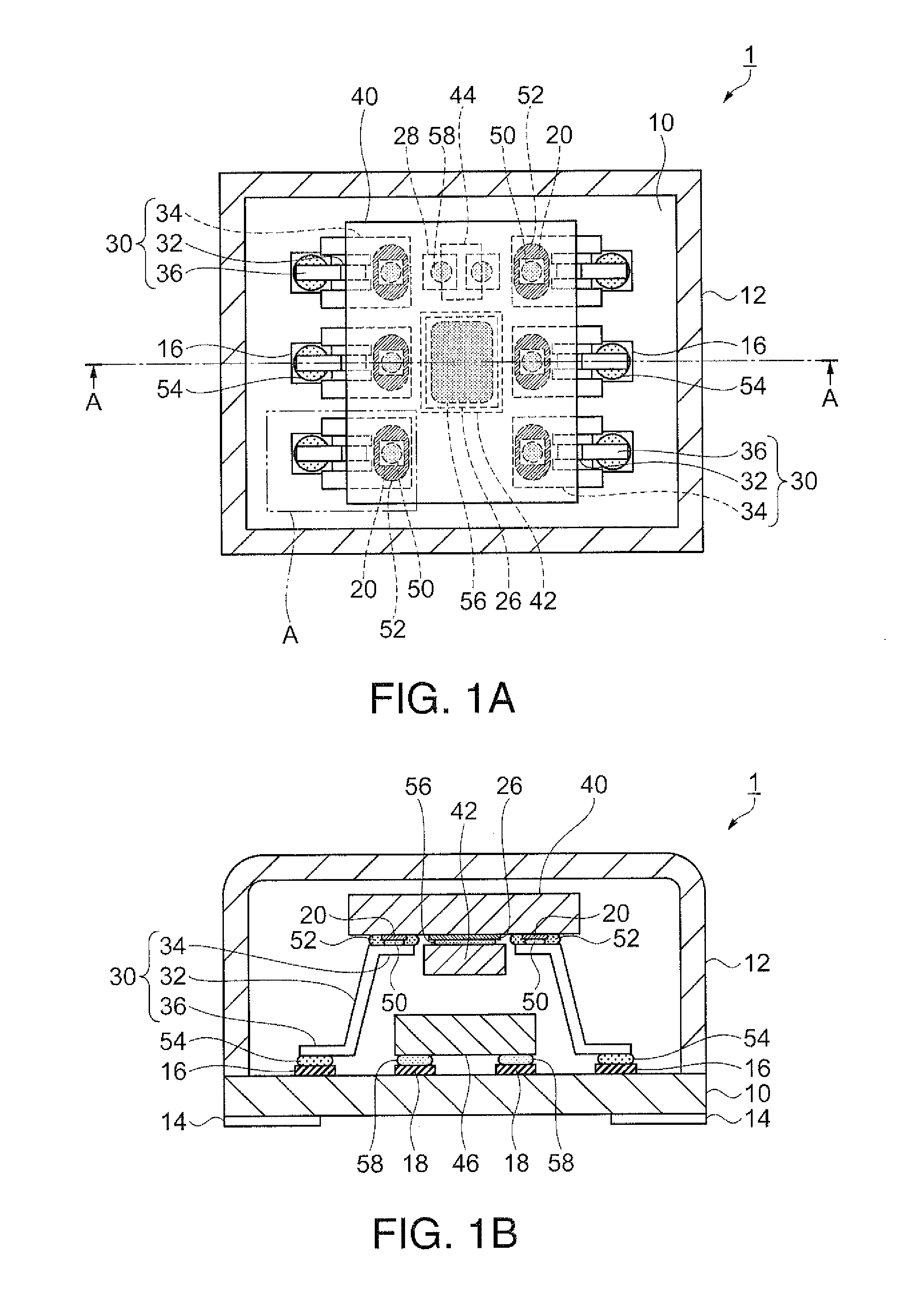
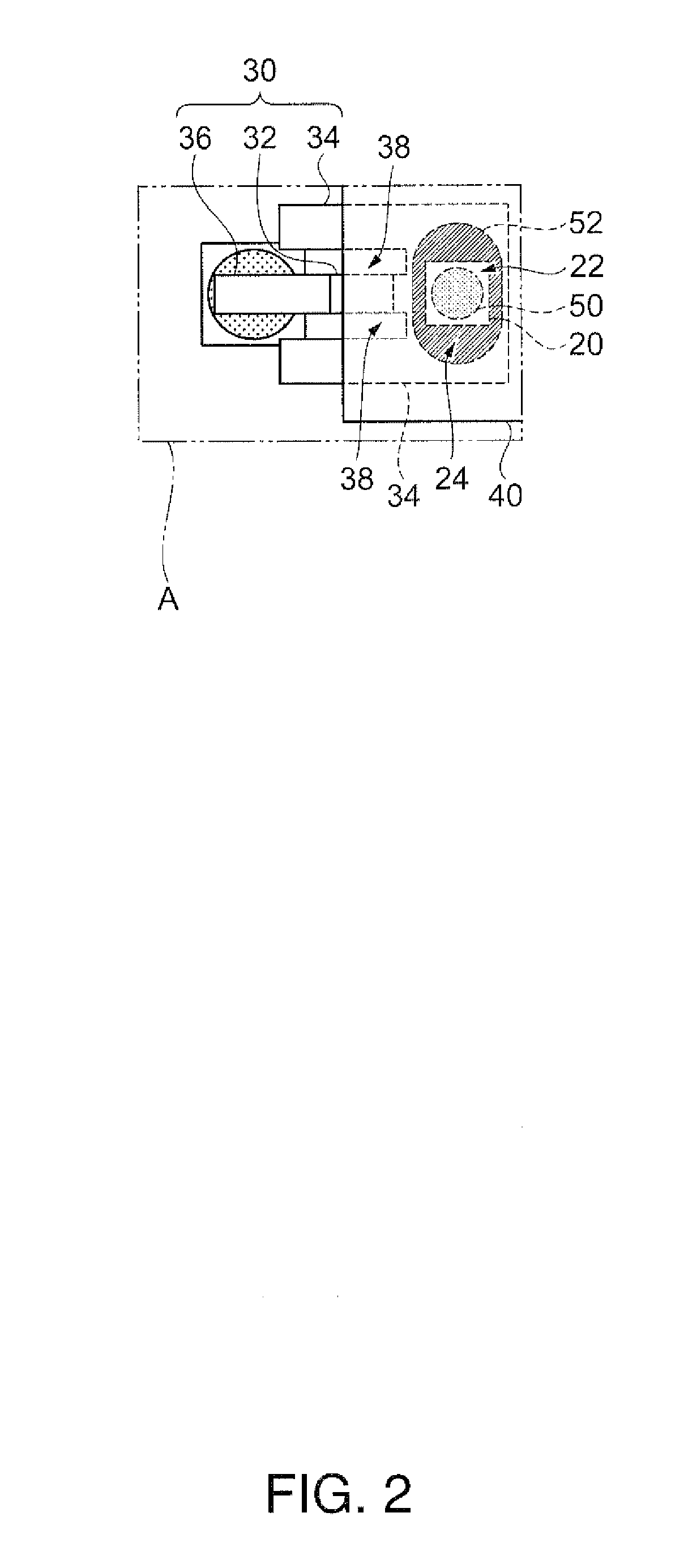
[0071]FIG. 10A is a schematic configuration view showing Modified Example 1 of the lead frame terminal used for the electronic device according to the embodiment of the invention.

[0072]Hereinafter, a lead frame terminal 30a of Modified Example 1 will be described mainly on the difference from the lead frame terminal 30 of the embodiment described above, and the description of the same matters is omitted.

[0073]As shown in FIG. 10A, the lead frame terminal 30a of Modified Example 1 differs from the lead frame terminal 30 of the embodiment in that each notch portion 38a disposed in a first terminal 34a has two widths, one on the side close to a second terminal 36a being large and the other on the side apart from the second terminal 36a being small.

[0074]With the configuration described above, since the fixing area between the first terminal 34a of the lead frame terminal 30a and an electronic component can be increased, there is an advantageous effect that the mechanical bonding streng...

modified example 2

[0075]FIG. 10B is a schematic configuration view showing Modified Example 2 of the lead frame terminal used for the electronic device according to the embodiment of the invention.

[0076]Hereinafter, a lead frame terminal 30b of Modified Example 2 will be described mainly on the difference from the lead frame terminal 30 of the embodiment described above, and the description of the same matters is omitted.

[0077]As shown in FIG. 10B, the lead frame terminal 30b of Modified Example 2 differs from the lead frame terminal 30 of the embodiment in that each notch portion 38b disposed in a first terminal 34b has two widths, one on the side close to a second terminal 36b being small and the other on the side apart from the second terminal 36b being large.

[0078]With the configuration described above, since the width of the notch portion 38b around a bent portion of the first terminal 34b is large, there is an advantageous effect that the first terminal 34b is easily bent in a direction apart f...

modified example 3

[0079]FIG. 10C is a schematic configuration view showing Modified Example 3 of the lead frame terminal used for the electronic device according to the embodiment of the invention.

[0080]Hereinafter, a lead frame terminal 30c of Modified Example 3 will be described mainly on the difference from the lead frame terminal 30 of the embodiment described above, and the description of the same matters is omitted.

[0081]As shown in FIG. 10C, the lead frame terminal 30c of Modified Example 3 differs from the lead frame terminal 30 of the embodiment in that a notch portion 38c is disposed in a first terminal 34c in a direction opposite to the side where a support portion 32c is coupled.

[0082]With the configuration described above, since the area of mounting an electronic component such as a heating element or a thermosensor on an electronic component connected with the lead frame terminal 30c can be increased, more other electronic components can be mounted. Therefore, there is an advantageous e...


PUM

PropertyMeasurementUnit
temperatureaaaaaaaaaa
frequency-stabilityaaaaaaaaaa
conductiveaaaaaaaaaa

Abstract

An electronic device includes: a support member including a first terminal, a second terminal, and a support portion extending from the first terminal and coupling the first terminal with the second terminal; an electronic component; and a bonding member connecting the first terminal with the electronic component. In a plan view along a direction in which the first terminal and the electronic component overlap each other, a portion of the first terminal is adjacent to the support portion with a notch portion therebetween and protrudes toward the extending direction side of the support portion. The support portion is bent at a portion adjacent to the protruding portion of the first terminal along the overlapping direction.

Description

BACKGROUND[0001]1. Technical Field[0002]The present invention relates to an electronic device, an electronic apparatus and a moving object in both of which an electronic device is mounted, and a method for manufacturing an electronic device.[0003]2. Related Art[0004]Heretofore, as electronic apparatuses are downsized and thinned, further downsizing and thinning are required for electronic devices mounted in the electronic apparatuses. Especially an electronic device, such as an oven controlled crystal oscillator (OCXO) having a structure in which the ambient temperature of a quartz crystal resonator is kept constant by heating with a heating element to avoid the influence of the ambient temperature for obtaining high frequency-stability, has a structure in which the heating element and the quartz crystal resonator are supported in a state of floating above a board using a support member to prevent an increase in power consumption due to the heat of the heating element conducting to ...

Claims


Application Information

Patent Timeline
Patent Type & Authority Applications(United States)
IPC IPC(8): H03L1/02H05K13/04H05K7/18
CPCH03L1/028H05K13/04H05K7/18H03L1/04H01L2224/16225H01L2924/16152Y10T29/49169H03H9/0552
Inventor KONDO, MANABU
Owner SEIKO EPSON CORP
Why Eureka
Try Eureka