Clamp for holding and efficiently removing heat from workpieces

a workpiece and heat transfer technology, applied in emergency protective circuit arrangements, coatings, chemical vapor deposition coatings, etc., can solve problems such as uneven cooling rate of gaseous heat conduction, poor heat transfer from workpiece to temperature controlled pedestal, condensation on parts of the pedestal exposed to atmospher

Inactive Publication Date: 2005-02-17
SAVAS STEPHEN EDWARD +1
View PDF14 Cites 54 Cited by
  • Summary
  • Abstract
  • Description
  • Claims
  • Application Information

AI Technical Summary

Problems solved by technology

Such low gas pressure in the narrow space between the wafer and the pedestal would result in poor heat transfer from workpiece to a temperature controlled pedestal.
This can cause problems including condensation on parts of the pedestal exposed to atmosphere and large temperature variations of the pedestal made of parts with different coefficients of thermal expansion.
In some cases there may be other problems including condensation of process reaction products on the pedestal.
In other cases where high heat removal and low substrate temperature is required, such a low pedestal temperatures might be required that coolant viscosity or chiller limitations would not permit it.
Heat needs to be removed uniformly from the wafer / substrate yet the structure on the surface will cause it to have an irregular spacing from the flat pedestal surface resulting in uneven rates of cooling by gaseous heat conduction when electrostatic clamping is used.
When the side of the wafer with devices on it is clamped to a hard surface high mechanical stresses may cause wafer breakage (especially for wafers that have been thinned by grinding) and / or surface damage.
Also, the presence of very small conducting structures on the clamped surface can lead to very high electric fields during electrostatic clamping which can cause electrical breakdown in the thin dielectric insulator covering the integrated circuit.
Such grinding, however, leaves IC's that have scratches in their backsides, which weakens them.
When such chips are mounted to a wiring board to make electronic products the stresses associated with the flexing of the board, or the thermal expansion of the board (when the IC's are in operation and producing heat) can cause the semiconductor material to break.
However, if the wafer material within the scratched and damaged layer is removed by a soft etching method then the strength of the wafer material is restored somewhat and the failure rate of the packaged IC's is much reduced.
When the wafer is very thin and / or fragile and the mechanical stresses on that material due to clamping of its irregular surface topography would be sufficient to cause damage or even breakage.
This damage is especially likely when a very thin wafer that has been ground down on the backside is being clamped.
In this case the stresses on the wafer when clamped to a hard surface would very likely be unacceptable.
Yet, such an elastomeric layer will become dirty or degrade in its function over time and by the etching of thousands of wafers or substrates, thereby necessitating frequent replacement.
In-situ cleaning processes might also degrade this layer, necessitating more frequent replacement or the spreading of elemental contamination which would compromise IC yields.
Further, small particles from the elastomer might become attached to the surface of the wafer or substrate and be difficult to remove from recessed spaces on the substrate surface.
Hard particles such as silicon dust will reduce the heat conduction from wafer to the elastomer and therefore need to be kept off the pedestal and wafer—which may not always be easy.
However, use of electrostatic clamping with such an elastomer is not used where a high rate of heat removal is required.
However, use of clamping Voltages of a kiloVolt or more will result in very high electric fields at the high points made of conducting materials.
This is likely to cause electrical breakdown in the elastomer or soft plastic.
Use of lower clamping voltages with such elastomers produces such modest clamping force (of order a fraction of a PSI) that this is inadequate to give good heat conduction from substrate to pedestal.
Use of a peripheral mechanical clamp is also not acceptable when very fragile substrates are being etched such as silicon wafers that have been ground down to less than 100 microns thickness or Gallium Arsenide wafers.
Typical electrostatic wafer clamping to the taped side of such wafers will not give effective thermal contact of the wafer with the pedestal due to the thickness of the dielectric layer, its low dielectric constant (normally less than 3.0) and the normal maximum of a kilo Volt for the clamping voltage.
The clamping pressure is too low.
In order to make such wafer clamping with significant pressure with a roughly 100 micron-thick plasma tape in between would require much higher clamping voltages than are typically employed, resulting in high likelihood of arcing or electrical breakdown of the dielectric layer or electrostatic damage to the IC.
Therefore, no previously existing technology is adequate for etching wafers or substrates at extremely high rates using RIE or other method having a high rate of wafer / substrate heating, while keeping wafer temperatures low.

Method used


Image

  • Clamp for holding and efficiently removing heat from workpieces
  • Clamp for holding and efficiently removing heat from workpieces

Examples


Embodiment Construction

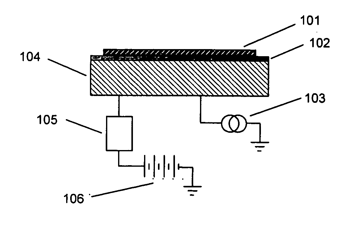
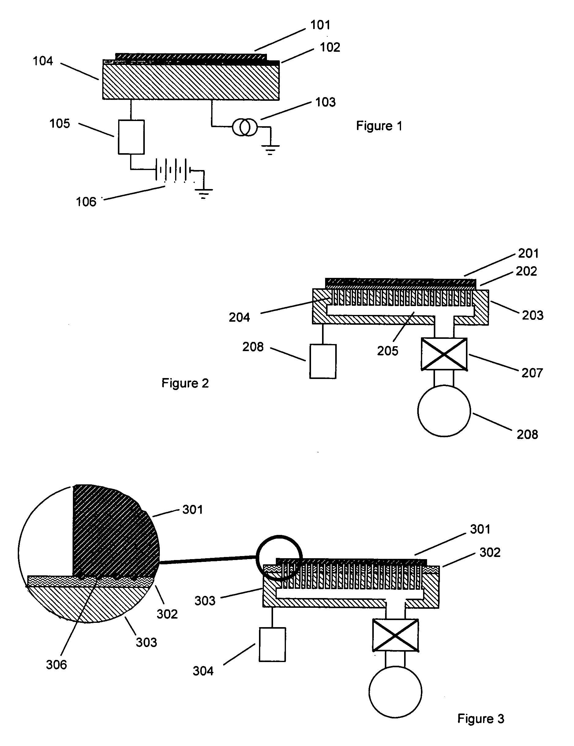
[0015] It is the object of the disclosed invention to effectively and safely clamp wafers or substrates to allow efficient heat transfer from them to a temperature controlled pedestal during plasma processing. This clamping system and method works with wafers or substrates that either have a soft plastic or elastomeric surface which completely covers one side, or that have a layer of such a soft plastic / elastomer applied to one side. In order to permit electrostatic clamping the soft or elastomeric layer should either be an electrical insulator or have very high electrical resistance. The clamping method employs a combination of vacuum and electrostatic pressure in sequence. Such clamping on the wafer or substrate causes the plastic or elastomeric material to conduct the heat from plasma processing efficiently from wafer or substrate to the temperature controlled pedestal thereby maintaining acceptably low wafer or substrate temperatures.

[0016] The pedestal to which wafers or subst...


PUM

PropertyMeasurementUnit
gas pressuresaaaaaaaaaa
voltageaaaaaaaaaa
temperatureaaaaaaaaaa

Abstract

The invention described in this disclosure is an apparatus and method for clamping semiconductor wafers or other substrates or workpieces during etching, CVD, or surface modification processes. The purpose of the invention is to achieve improved heat transfer during processing between the wafer/substrate and a temperature controlled pedestal used for supporting it in the process chamber. The typical level of process heat put into the wafer during plasma-based etching or deposition processes will be up to about 10 Watts per centimeter squared while the maximum acceptable temperature differential between wafer/substrate and pedestal is less than about 100 Celsius. In such low gas pressure environments typical for plasma-based processes, the heat removal from the wafer/substrate by gaseous conduction may be inadequate to meet requirements. This invention achieves excellent heat transfer to the pedestal from the wafer/substrate when there is a thin, resilient, electrically insulating layer (tape) bonded to the wafer/substrate or the pedestal. Wafer/substrate clamping for improved process heat removal is achieved by a combination of vacuum clamping of the wafer/substrate beginning prior to evacuation of the processing chamber, along with or followed by electrostatic clamping of the wafer/substrate which continues during processing. The invention also permits the wafer/substrate to be rapidly and safely released from the electrostatic clamping when the chamber is returned to atmospheric pressure by a providing a slight pressure increase, above atmospheric pressure, between wafer and pedestal. The pedestal may have some roughening or narrow grooves on the wafer clamping surface, and some small holes from its surface leading to an evacuated plenum or channel within the pedestal. Alternatively, the pedestal may have a layer of a porous metal extending from its surface down to the evacuated channel or plenum which permits gas to be evacuated. These structures allow vacuum pumping of gas that might otherwise be trapped between the insulating layer and the pedestal. When a wafer/substrate is placed on the pedestal by loading at atmospheric pressure, vacuum pumping through the pedestal is commenced. This causes the workpiece to be pressed to the pedestal clamping surface with approximately atmospheric pressure compressing the soft layer against its clamping surface. This provides sufficient contact of the soft layer with the pedestal to greatly improve heat transfer from the wafer/substrate to the pedestal. A voltage is applied to the pedestal, beginning any time after the wafer is on the pedestal, to further clamp the wafer electrostatically. As the processing chamber is then pumped down to operating pressure for processing the electrostatic clamping voltage maintains sufficient pressure of the wafer/substrate against the pedestal to maintain the heat conductive contact between the soft layer and the pedestal. This permits good heat conduction to be maintained during the low pressure plasma-based etching or CVD processing. Following processing when the wafer/substrate is to be removed it may be rapidly de-clamped from the electrostatic clamping by application of a slight over-atmospheric pressure in the reservoir or pumping channels within the pedestal.

Description

RELATED APPLICATION [0001] This application is based upon Provisional Application No. 60 / 472,354, filed May 20, 2003, the priority of which is claimed.BACKGROUND OF THE INVENTION [0002] 1. Field of Invention [0003] This invention pertains generally to the processing of semiconductor wafers and, more particularly, to a clamp for holding workpieces so that process heat removal is efficient and consistent. [0004] 2. Related Art [0005] Typically, wafers / substrates are electrostatically clamped during many plasma-based Fabrication processes, such as etching or CVD, to facilitate heat transfer between the wafer / workpiece and the support pedestal. This is particularly the case in processing of semiconductor wafers to make large scale integrated circuits where process heat normally needs to be removed from the wafer. It is also the case in processing substrates for flat panel displays. Normally, in these technologies up to about two to three Watts per centimeter squared of process heat need...

Claims


Application Information

Patent Timeline
Patent Type & Authority Applications(United States)
IPC IPC(8): C23C16/458H01L21/683H01L21/687
CPCC23C16/4586H01L21/68707H01L21/6838H01L21/6831
Inventor SAVAS, STEPHEN EDWARDZAJAC, JOHN
Owner SAVAS STEPHEN EDWARD
Why Eureka
Try Eureka