Optimal bank height for inkjet printing

a technology of inkjet printing and bank height, which is applied in the direction of semiconductor devices, electrical devices, organic semiconductor devices, etc., can solve the problems of uniform and concave drying patterns, affecting the shape of the film, and the pockets formed by the photo-resist bank can often affect the spreading/flow/drying, so as to prevent any spillage of liquid and uniform drying profiles

Active Publication Date: 2005-07-14
DOLYA HOLDCO 5 LTD
View PDF3 Cites 27 Cited by
  • Summary
  • Abstract
  • Description
  • Claims
  • Application Information

AI Technical Summary

Benefits of technology

[0017] In accordance with the invention, the height of the photo-resist layer “banks” which define pockets for inkjet printing or other patterned processes are optimized to provide a more uniform drying profile for substances which are to be deposited in those pockets and then dried therein. Preferably, the height of the banks is under three microns in height, while tall enough to prevent any spillage of liquid over the banks. In some embodiments of the invention, the height of the mushroom banks is set to be one micron or less.

Problems solved by technology

In the case of selective deposition such as inkjet printing, however, pockets that are formed by photo-resist banks can often affect the spreading / flow / drying and affect the shape of the film.
While spin coating of polymers may be appropriate for monochrome light emission, it is generally not used when a pattern of pixels of different colors is desired.
(although it is possible to deposit a different material from each nozzle, industrial printers are not designed like that.
However high photo-resist banks can lead to non-uniform and concave drying patterns.
The profile, when dried from a liquid drop, will not be very flat or uniform.
There is pileup at the edges which affects the useful part of the device.
In addition the higher current density in the thinner part of the film would lead to faster degradation of the sample and hence a shorter lifetime of the device / product.

Method used


Image

  • Optimal bank height for inkjet printing
  • Optimal bank height for inkjet printing
  • Optimal bank height for inkjet printing

Examples


Embodiment Construction

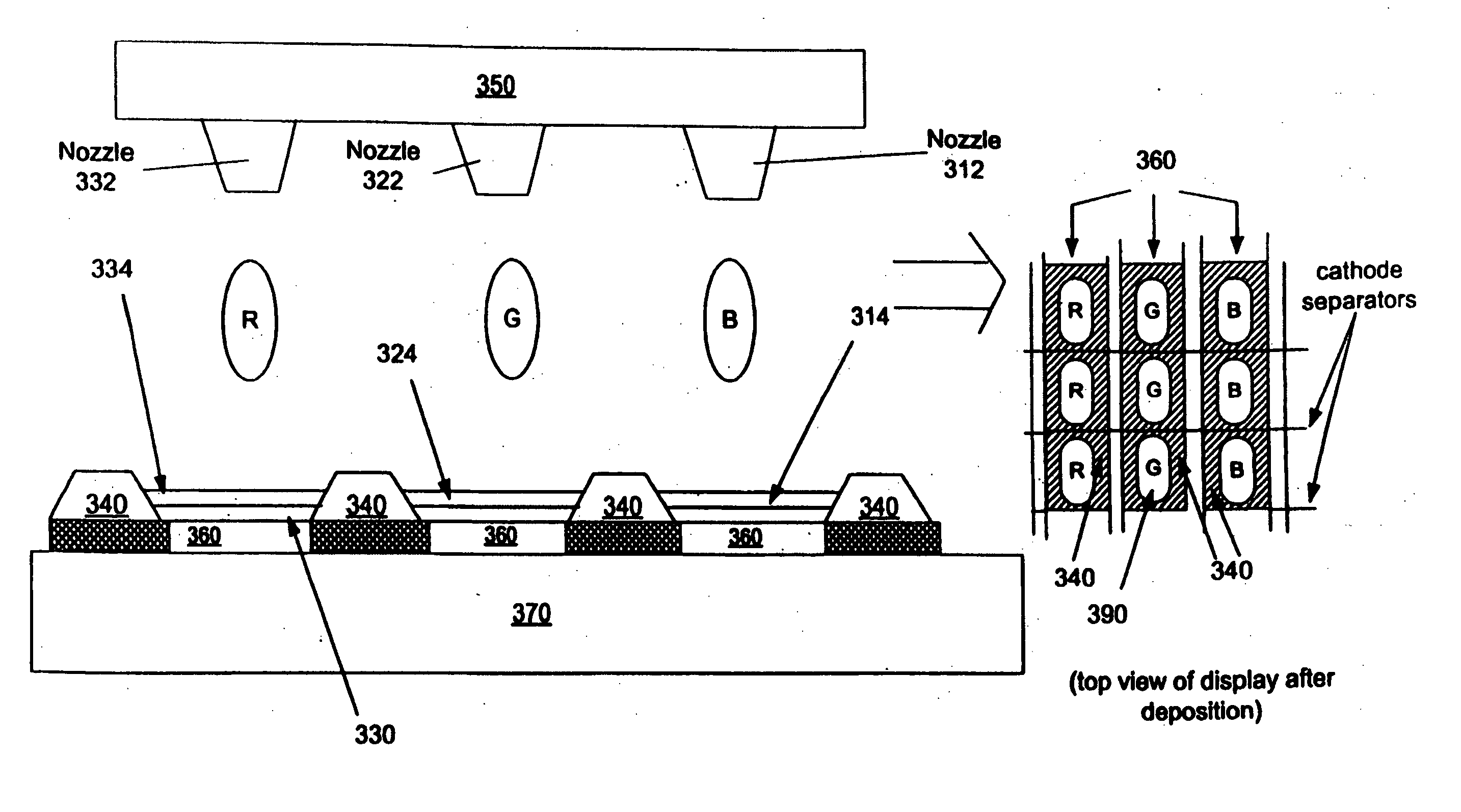
[0025] In accordance with the invention, the height of the photo-resist layer “banks” which define pockets for inkjet printing or other patterned processes are optimized to provide a more uniform drying profile for substances which are to be deposited in those pockets. Preferably, the height of the banks are less than three microns, and more preferably, down to a height of one micron. A lower bank height reduces the level of build-up on and near the walls of the banks and induces a more uniform and flatter profile when a substance dropped into a pocket is allowed to dry.

[0026] The amount of substance deposited within the banks, as well as the composition (properties) of the deposited substance contribute to the drying profile and thus, are factors in determining the optimal height of the photo-resist banks. In addition, the materials used in constructing the banks and surface treatments on the lower electrode layer and the photo-resist bank layer (or already deposited polymer layer...


PUM


Abstract

The height of the photo-resist layer “banks” which define pockets for inkjet printing or other patterned processes is optimized to provide a more uniform drying profile for substances which are to be deposited in those pockets and dried therein. Preferably, the height of the photo-resist layer is less than or equal to about three microns and more, preferably, about one micron.

Description

BACKGROUND [0001] 1. Field of the Invention [0002] This invention relates generally to the art of thin film device processing and fabrication. More specifically, the invention relates to the fabrication of Organic Light Emitting Diode based displays and other electronic devices which use selective deposition. [0003] 2. Related Art [0004] Display and lighting systems based on LEDs (Light Emitting Diodes) have a variety of applications. Such display and lighting systems are designed by arranging a plurality of opto-electronic elements (“elements”) such as arrays of individual LEDs. LEDs that are based upon semiconductor technology have traditionally used inorganic materials, but recently, the organic LED (“OLED”) has come into vogue for certain applications. Examples of other elements / devices using organic materials include organic solar cells, organic transistors, organic detectors, and organic lasers. There are also a number of bio-technology applications such as biochips for DNA re...

Claims


Application Information

Patent Timeline
Patent Type & Authority Applications(United States)
IPC IPC(8): H01L21/00H01L27/32H01L51/00
CPCH01L27/3211H01L27/3246H01L2251/558H01L51/0005H01L27/3283H10K59/35H10K59/122H10K59/173H10K71/135H10K2102/351
Inventor GUPTA, RAHULINGLE, ANDREWNATARAJAN, SRIRAM
Owner DOLYA HOLDCO 5 LTD
Why Eureka
Try Eureka