Tap sampling at double rate

Active Publication Date: 2005-07-28
STMICROELECTRONICS RES & DEV
View PDF12 Cites 20 Cited by
  • Summary
  • Abstract
  • Description
  • Claims
  • Application Information

AI Technical Summary

Benefits of technology

[0019] To address the above-discussed deficiencies of the prior art, it is an aim of embodiments of the invention to address one or more of these problems
[0020] According to one aspect of the invention there is provided an integrated circuit comprising: at least one test input for receiving test data; test control circuitry between said at least one test input and circuitry to be tested; wherein said

Problems solved by technology

Nowadays, chips are more complex and contain not only a processor on-chip but also its associated memory and other ancillary circuitry.
Thus, it is no longer a simple matter to monitor the operation of the processor because the signals which are normally available off-chip no longer provide a direct indication as to the internal operation of the CPU(s).
Even where it is not practical or not possible to achieve non-intrusive monitoring, there is still a requirement to gain access to the operation of software being executed on a plurality of CPUs on-chip with the minimum of intrusion.
However,

Method used


Image

  • Tap sampling at double rate
  • Tap sampling at double rate
  • Tap sampling at double rate

Examples


Embodiment Construction

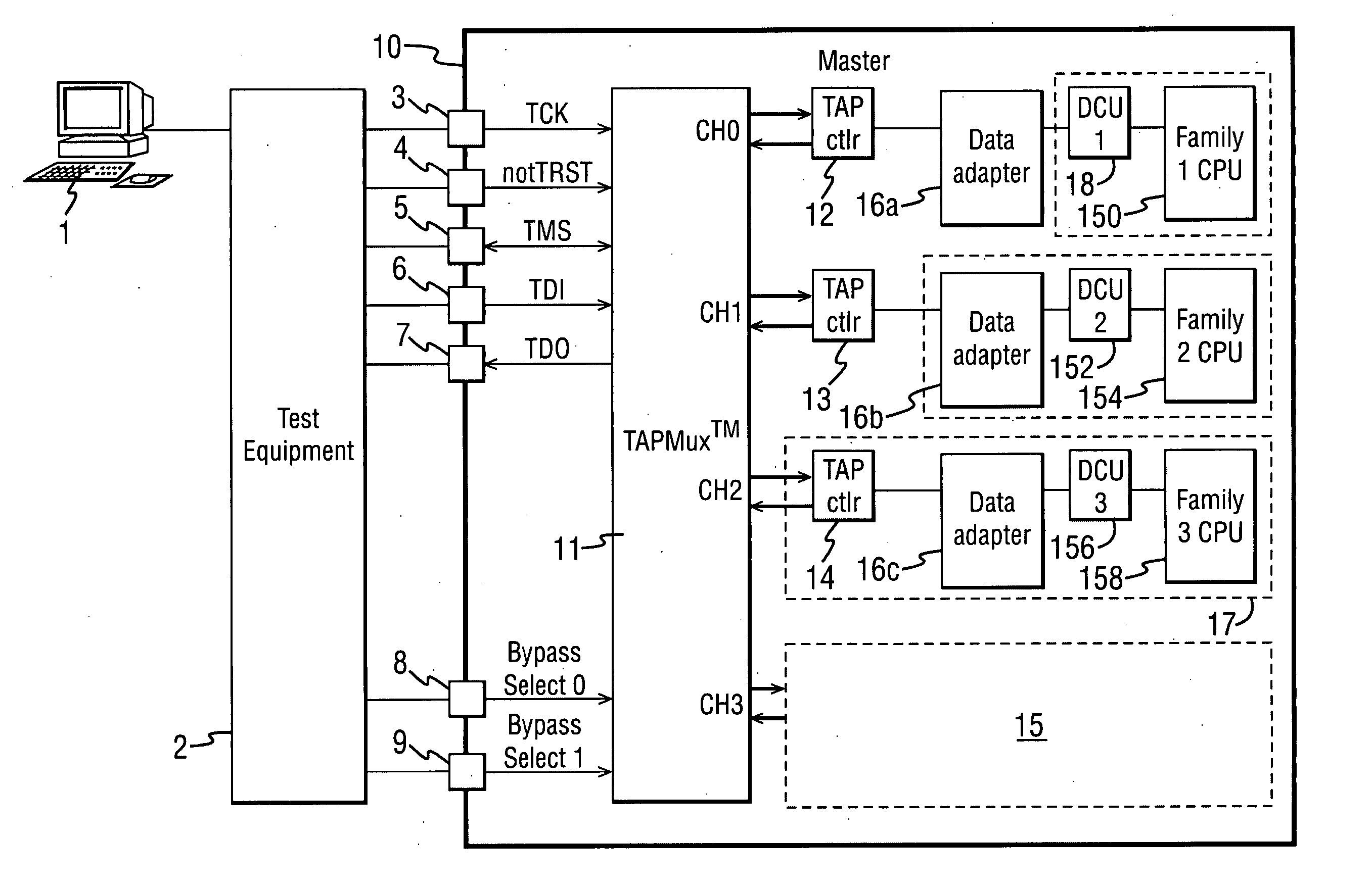
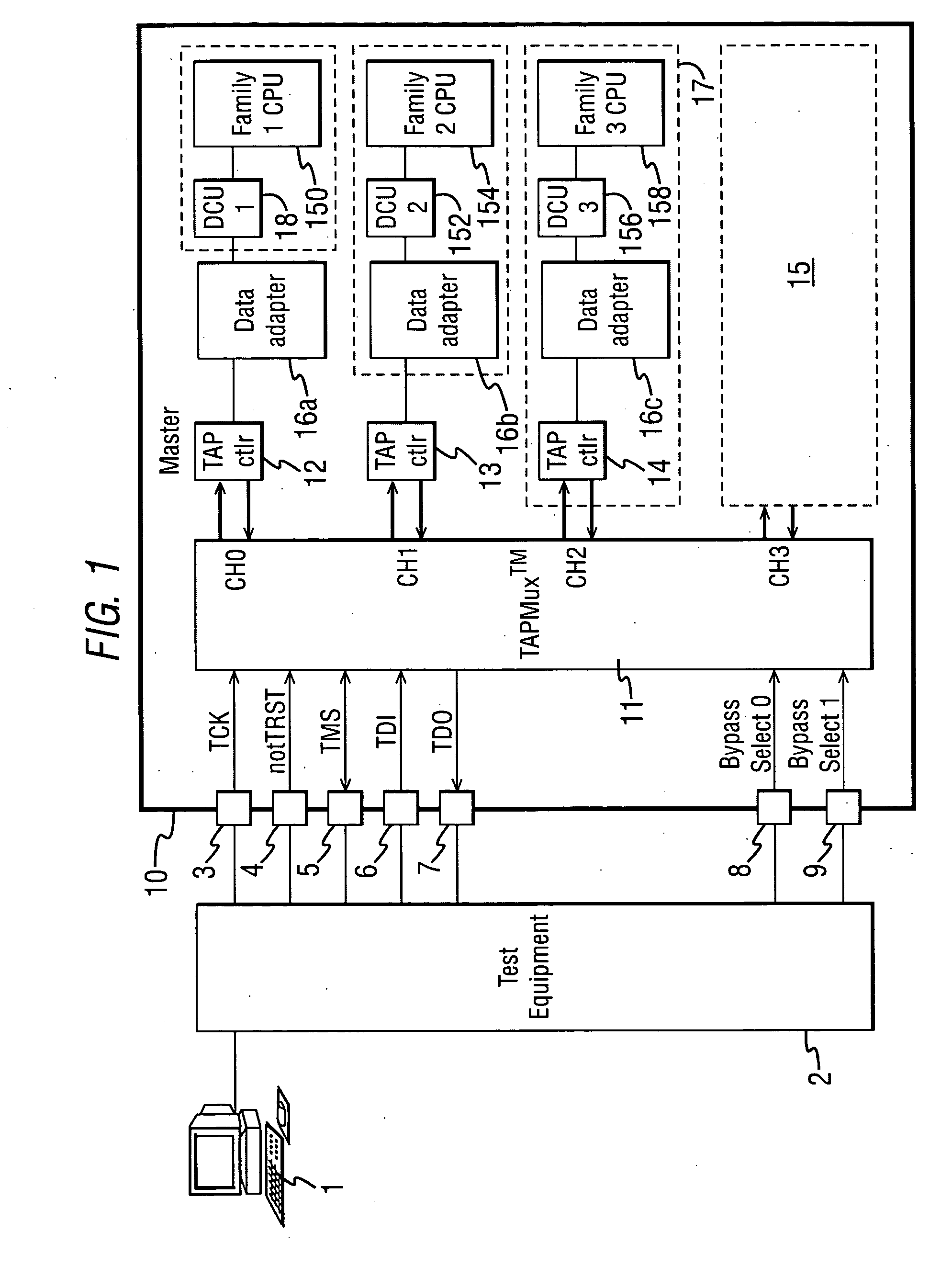
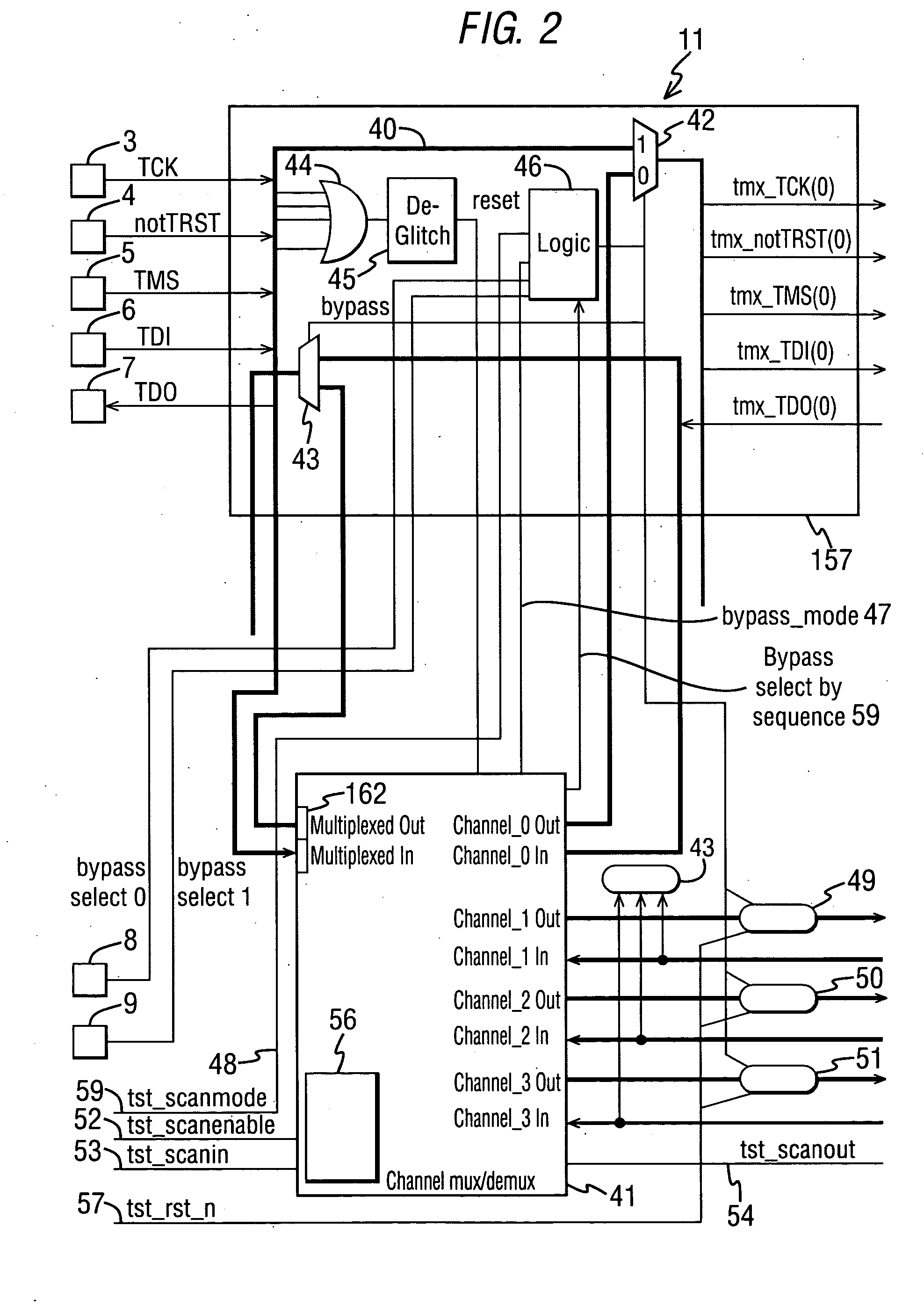
[0043]FIGS. 1 through 17b, discussed below, and the various embodiments used to describe the principles of the present invention in this patent dolcument are by way of illustration only and should not be construed in any way to limit the scope of the invention. Those skilled in the art will understand that the principles of the present invention may be implemented in any suitably arranged integrated circuit having at least one test input.

[0044]FIG. 1 illustrates schematically an embodiment of the present invention. A host computer 1 is connected to test equipment 2 which is in turn connected to external pins 3-9 on an integrated circuit or chip 10. The integrated circuit 10 receives from the test equipment 2 a test clock input TCK on pin 3, a test reset input notTRST on pin 4, a test mode select input TMS on pin 5, a test data input TDI on pin 6, a first channel select input BYPASS_SELECT0 on pin 8 and a second channel select input BYPASS_SELECT1 on pin 9. The bypass select pins ma...


PUM


Abstract

An integrated circuit comprising: at least one test input for receiving test data; test control circuitry between the at least one test input and circuitry to be tested; wherein the test data is clocked in on a rising clock edge and a falling clock edge.

Description

CROSS-REFERENCE TO RELATED APPLICATIONS [0001] The present invention is related to those disclosed in the following U.S. Non-Provisional Patent Applications: [0002] 1) [Docket No. STMI08-00009] filed concurrently herewith, entitled “TAP MULTIPLEXER”. [0003] 2) [Docket No. STMI08-00010] filed concurrently herewith, entitled “TAP TIME DIVISION MULTIPLEXING”; [0004] 3) [Docket No. STMI08-00011] filed concurrently herewith, entitled “TAP TIME DIVISION MULTIPLEXING WITH SCAN TEST”; and The above applications are commonly assigned to the assignee of the present invention. The disclosures of these related patent applications are hereby incorporated by reference for all purposes as if fully set forth herein.TECHNICAL FIELD OF THE INVENTION [0005] This invention relates to an integrated circuit. BACKGROUND OF THE INVENTION [0006] Test access port (TAP) controllers are known in the art. TAP controllers are used to effect communication of test data on and off chip via what is known as a JTAG ...

Claims


Application Information

Patent Timeline
IPC IPC(8): G01R31/3185G01R31/3187
CPCG01R31/318536G01R31/318552G01R31/3187G01R31/318558G01R31/318563G01R31/318555
Inventor WARREN, ROBERT
Owner STMICROELECTRONICS RES & DEV
Why Eureka
Try Eureka