Semiconductor device

a technology of semiconductor devices and capacitors, applied in semiconductor devices, semiconductor/solid-state device details, electrical apparatus, etc., can solve the problems of cap film not being formed as desired on each of the low dielectric constant films, cap film tending to incur damage, and subsequent process steps

Inactive Publication Date: 2005-08-04
KK TOSHIBA
View PDF6 Cites 72 Cited by
  • Summary
  • Abstract
  • Description
  • Claims
  • Application Information

AI Technical Summary

Problems solved by technology

Also, if dust or small cracks are present in the low dielectric constant film, the cap film may fail to be formed as desired on each of the low dielectric constant films.
In this case, the cap film tends to incur damage in the subsequent process steps.
The conventional multi-layered wiring structure gives rise to another problem.
The water and the gas bring about problems in the subsequent process steps.
Also, the low dielectric constant film cannot be formed and processed as desired.
Further, a good resolution of the pattern cannot be obtained in the low dielectric constant film.
Therefore, the gas is not dissipated sufficiently in the portion where the plug density is low, i.e., in the low dielectric constant film with few openings.
Problems attributed to the gas are highly likely to arise in this area.

Method used


Image

  • Semiconductor device
  • Semiconductor device
  • Semiconductor device

Examples


first embodiment

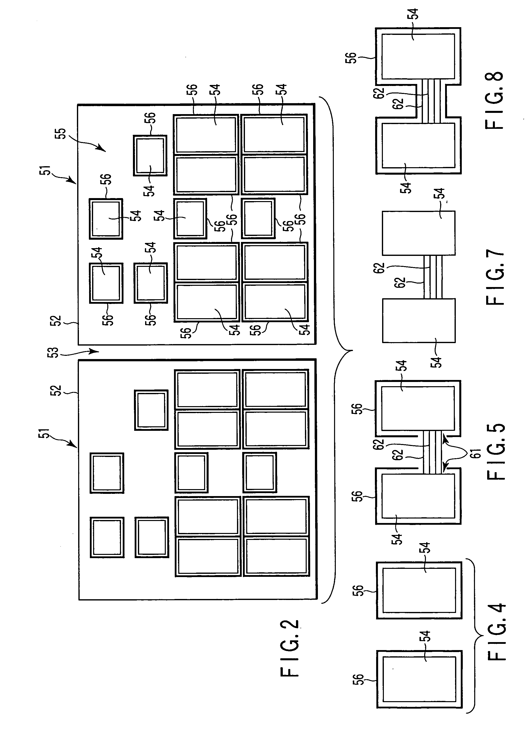
[0063]FIG. 2 is a plan view schematically showing the construction of a semiconductor device according to a first embodiment of the present invention. As shown in FIG. 2, semiconductor chips 51 (two are shown as an example) are formed on a main surface of the semiconductor substrate 1. Each of the semiconductor chips 51 is surrounded by a fence (chip ring) 52 (element protective member). To be more specific, the fence 52 extends on a plane (horizontal plane) parallel to the main surface of the semiconductor substrate 1 so as to surround continuously the device region (element region) corresponding to the semiconductor chip 51. Also, a dicing line (dicing region) 53 is formed around the semiconductor chip 51.

[0064] Functional circuit blocks 54 are formed within the semiconductor chip 51. Each of the functional circuit blocks 54 performs a properly independent function and corresponds to, for example, the macro (core) of the system LSI (Large Scale Integrated circuit). A boundary reg...

second embodiment

[0074] A second embodiment is employed in combination with the first embodiment. In the second embodiment, the fence 56 is partly discontinuous in the wiring level of a high layer. Alternatively, the fence 56 is not formed in the high layer.

[0075]FIGS. 4 and 5 are plan views each showing schematically the construction of a part of a semiconductor device according to the second embodiment of the present invention. As shown in FIGS. 4 and 5, the semiconductor device comprises, for example, substantially three wiring levels. To be more specific, a second wiring level and a third wiring level are formed successively on a first wiring level constituting the lowermost wiring level. The interlayer insulating film in each of the first and second wiring levels consists of a low-k material. On the other hand, the interlayer insulating film in the third wiring level consists of a non low-k material. It is possible to form the first to third wiring levels as respective first to third wiring le...

third embodiment

[0081] A third embodiment is an application of the second embodiment. In the third embodiment, the fence 56 also surrounds the block connecting wiring 62.

[0082]FIG. 8 is a plan view schematically showing the construction of a semiconductor device according to the third embodiment. As shown in FIG. 8, the fence 56 continuously surrounds collectively the functional circuit blocks 54 connected to each other by the wiring 62 and the block connecting wiring 62 in the third wiring level. The constructions of the first wiring level 63 and the second wiring level 64 remain unchanged from the second embodiment.

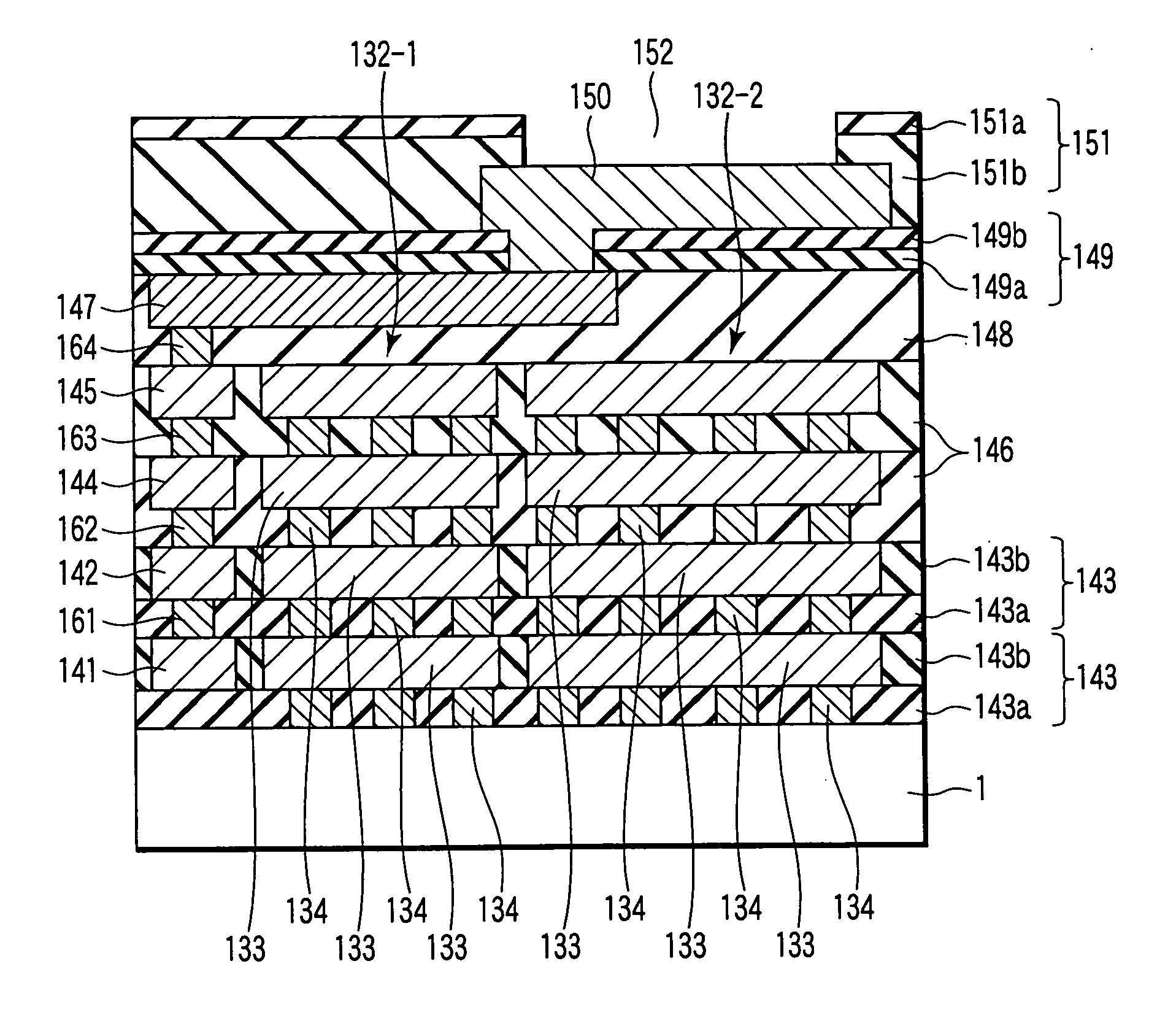
[0083] In the semiconductor device according to the third embodiment, it is possible to obtain the same effect as in the second embodiment. Further, the fence 56 does not have an opening, so as to form a closed structure in the third wiring level 65. Therefore, the water and the gas permeating into the interlayer insulating film of the third wiring level 65 can be it is possible to p...


PUM


Abstract

A semiconductor device includes a first insulating layer provided above a semiconductor substrate. The first insulating layer includes a layer consisting essentially of a material having a relative dielectric constant smaller than 3. The first insulating layer includes a first integral structure consisting of a plug and wiring. The upper surface of the wiring is flush with the upper surface of the first insulating layer, and the lower surface of the plug is flush with the lower surface of the first insulating layer. A region protective member is formed of a second integral structure consisting of a plug and wiring. The second integral structure extends from the upper surface of the first insulating layer to the lower surface of the first insulating layer. The region protective member surrounds one of first to n-th regions (n being a natural 2 or more) partitioned by a boundary region on a horizontal plane.

Description

CROSS-REFERENCE TO RELATED APPLICATIONS [0001] This application is based upon and claims the benefit of priority from the prior Japanese Patent Applications No. 2004-8303, filed Jan. 15, 2004 and No. 2004-195731, filed Jul. 1, 2004, the entire contents of both of which are incorporated herein by reference. BACKGROUND OF THE INVENTION [0002] 1. Field of the Invention [0003] The present invention relates to a semiconductor device, particularly, to the construction and arrangement of a dummy pattern included in a multi-layered wiring structure using, for example, a material having a low relative dielectric constant. [0004] 2. Description of the Related Art [0005]FIG. 24 is a plan view showing a semiconductor device having the conventional multi-layered wiring structure. FIG. 25 is a sectional view taken along the line XXV-XXV shown in FIG. 24. As FIGS. 24 and 25 show, a chip ring 103, which is also referred to as a via ring, a crack stopper, a metal ring or a metal fence, is formed in ...

Claims


Application Information

Patent Timeline
Patent Type & Authority Applications(United States)
IPC IPC(8): H01L23/52H01L21/00H01L21/3205H01L21/822H01L23/00H01L23/522H01L23/58H01L27/04H01L27/10H01L29/40
CPCH01L23/522H01L23/564H01L23/585H01L2924/0002H01L2924/00
Inventor NAKAMURA, NAOFUMIMATSUNAGA, NORIAKIITO, SACHIYOHASUNUMA, MASAHIKONISHIOKA, TAKESHI
Owner KK TOSHIBA
Why Eureka
Try Eureka