
Semiconductor memory device which stores plural data in a cell

a memory device and memory technology, applied in the field of semiconductor memory devices, can solve the problems of long time to carry and difficulty in speeding up data write operations

Active Publication Date: 2005-08-04
KIOXIA CORP
View PDF19 Cites 200 Cited by
  • Summary
  • Abstract
  • Description
  • Claims
  • Application Information

AI Technical Summary

Benefits of technology

[0013] According to a fifth aspect of the present intention, there is provided a semiconductor memory device comprising: a memory which stores at least one data item; at least one data storage circuit which is connected to the memory cell and stores externally inputted data of a first logic level or a second logic level; and a control circuit which controls the operation of the data storage circuit, wherein the control circuit, when the logic level of the data stored in the data storage circuit is the first logic level, inverts the logic level to the second logic level and, when the logic of the data is the second logic level, inverts the logic level to the first logic level and further, when the logic level of the data stored in the data storage circuit is the first logic level, does writing on the memory cell to raise the threshold voltage and, when the logic level of the data is the second level, causes the threshold voltage of the memory cell to remain unchanged.

Problems solved by technology

Consequently, it requires a long time to carry out the verify operation, which makes it difficult to speed up the data write operation.

Method used


Image

  • Semiconductor memory device which stores plural data in a cell
  • Semiconductor memory device which stores plural data in a cell
  • Semiconductor memory device which stores plural data in a cell

Examples


first embodiment

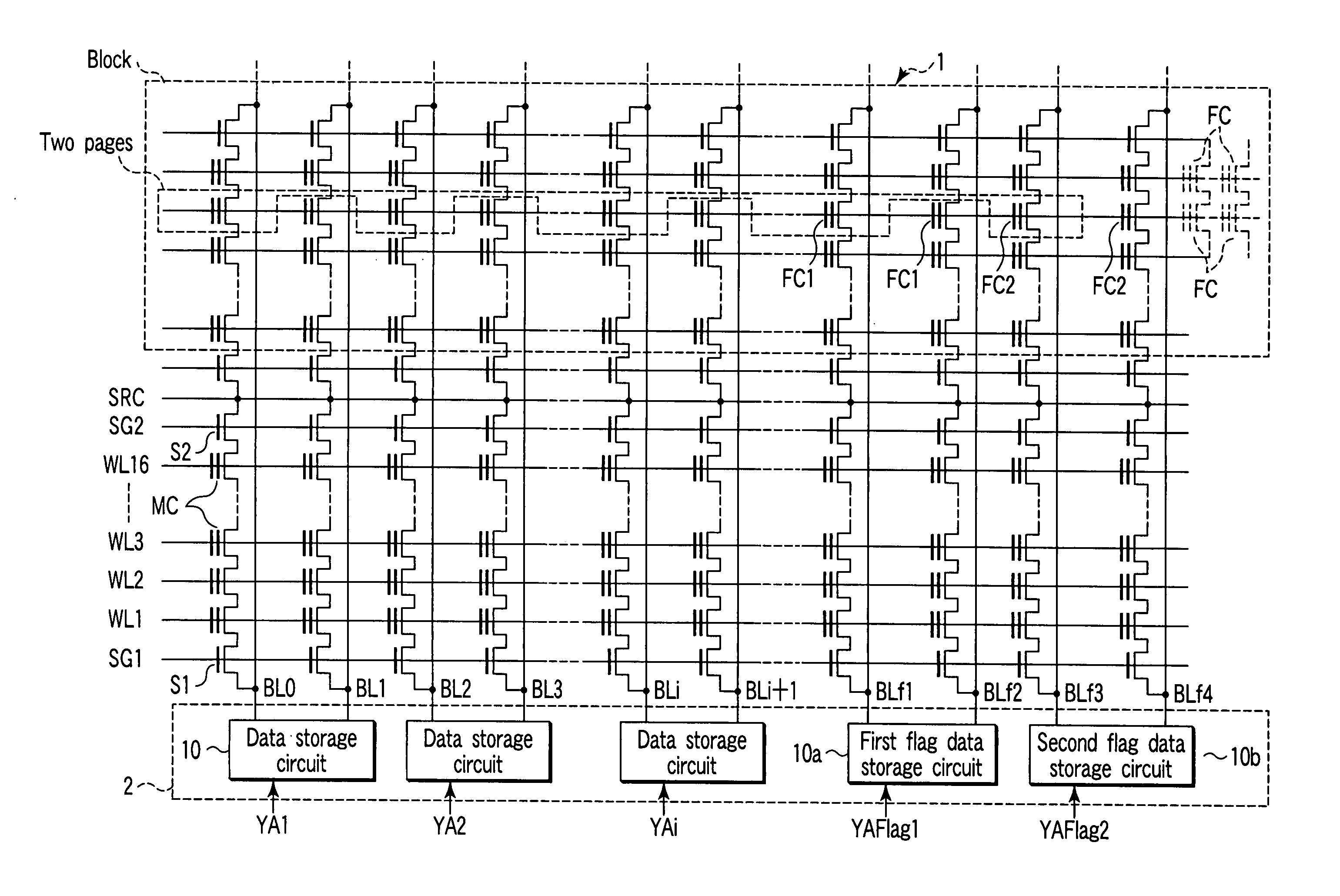
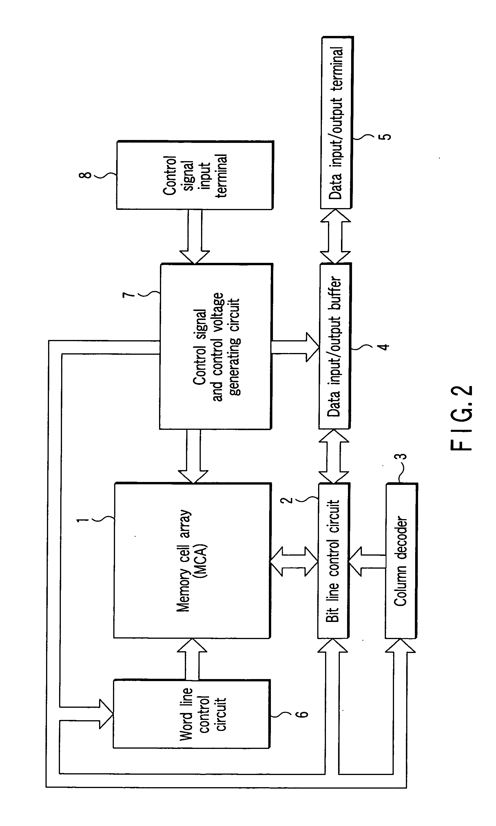
[0087]FIG. 2 schematically shows the configuration of a nonvolatile semiconductor memory device according to a first embodiment of the present invention. For example, the configuration of a NAND flash memory which stores 4-valued (2 bits of) data is shown in FIG. 2.

[0088] A memory cell array 1 includes a plurality of bit lines, a plurality of word lines, and a common source line. In the memory array 1, for example, memory cells are arranged in a matrix. Each of the memory cells is composed of an EEPROM cell and enables data to be rewritten electrically. A bit line control circuit 2 for controlling the bit lines and a word line control circuit 6 are connected to the memory cell array 1.

[0089] The bit line control circuit 2 includes a plurality of data storage circuits and a flag data storage circuit as described later. The bit line control circuit 2 reads the data in a memory cell in the memory cell array 1 via a bit line, detects the state of a memory cell in the memory cell array...

second embodiment

[0262]FIG. 19 shows a memory cell array 1 and a bit line control circuit 2 in a NAND flash memory for storing 8-valued (3 bits of) data according to a second embodiment of the present invention. Since the configuration of FIG. 19 is almost the same as the configuration for 4-valued (2 bits of) data shown in FIG. 3, only the part differing from the configuration of FIG. 3 will be explained.

[0263] In FIG. 19, when one word line is selected by an external address, then one sector shown by a broken line is selected. One sector is composed of three pages. An address is used to switch between the three pages. Specifically, since 3 bits of data can be stored in a memory cell, the switching between three bits is done by an address (a first page, a second page, and a third page). One sector has five flag cells FC1, FC2, FC3, FC4, and FC5 (FIG. 19 shows only flag cells FC1 and FC5). Therefore, when one word line is selected, the five flag cells FC1, FC2, FC3, FC4, and FC5 are selected at the...

third embodiment

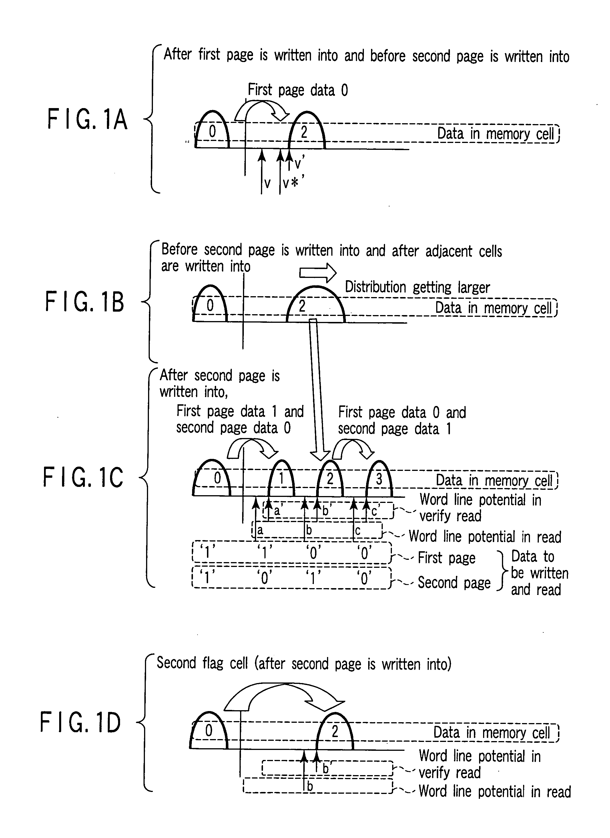
[0353] In the second embodiment, the flag cells FC1 to FC5 have written into as follows. When the second page is written into, the flag cell FC1 is written into to the verify potential “b*′” and the flag cell FC2 is written into to the verify potential “d*′”. When the third page is written into, the flag cell FC3 is written into to the verify potential “a′”, the flag cell FC4 is written into to the verify potential “b′”, and the flag cell FC5 is written into to the verify potential “d′”. For this reason, the second embodiment uses five flag cells. However, the flag cell FC1 can be substituted for the flag cell FC4 and the flag cell FC2 can be substituted for the flag cell FC5. Therefore, the circuit shown in FIG. 19 can be composed of three flag data storage circuits and three flag cells FC1, FC2, and FC3.

[0354] In the above configuration, the first and second page write operations are the same as in the second embodiment. The third page write operation differs a little from that i...


PUM


Abstract

A memory cell array is configured to have a plurality of memory cells arranged in a matrix, each of the memory cells being connected to a word line and a bit line and being capable of storing n values (n is a natural number equal to or larger than 3). A control circuit controls the potentials of the word line and bit line according to input data and writes data into a memory cell. The control circuit writes data into the memory cell to a k-valued threshold voltage (k<=n) in a write operation, precharges the bit line once, and then changes the potential of the word line an i number of times to verify whether the memory cell has reached an i-valued (i<=k) threshold voltage.

Description

CROSS-REFERENCE TO RELATED APPLICATIONS [0001] This application is based upon and claims the benefit of priority from prior Japanese Patent Applications No. 2004-024475, filed Jan. 30, 2004; and No. 2004-160165, filed May 28, 2004, the entire contents of both of which are incorporated herein by reference. BACKGROUND OF THE INVENTION [0002] 1. Field of the Invention [0003] This invention relates to a semiconductor memory device capable of storing, for example, 2 bits or more of data. [0004] 2. Description of the Related Art [0005] A nonvolatile semiconductor memory device capable of storing multivalued data, such as a NAND flash memory using EEPROM, has been proposed (for example, refer to Jpn. Pat. Appln. KOKAI Publication No. 2000-195280). [0006] In a nonvolatile semiconductor memory device of this type, when multivalued data is stored in a memory cell, a threshold voltage corresponding to each data is set in the memory cell. The number of threshold voltages increases as the number...

Claims


Application Information

Patent Timeline
IPC IPC(8): G11C11/34G11C16/02G11C11/56G11C16/04G11C16/06G11C16/12G11C16/34
CPCG11C11/5628G11C16/0483G11C16/12G11C16/10G11C16/3459G11C2211/5621G11C2211/5648G11C16/3454G11C16/04G11C11/5642
Inventor SHIBATA, NOBORUTANAKA, TOMOHARU
Owner KIOXIA CORP
Features
  • Generate Ideas
  • Intellectual Property
  • Life Sciences
  • Materials
  • Tech Scout
  • Unparalleled Data Quality
  • Higher Quality Content
  • 60% Fewer Hallucinations
Learn More