Thin semiconductor chip manufacturing method
- Summary
- Abstract
- Description
- Claims
- Application Information
AI Technical Summary
Benefits of technology
Problems solved by technology
Method used
Image

Examples
first embodiment
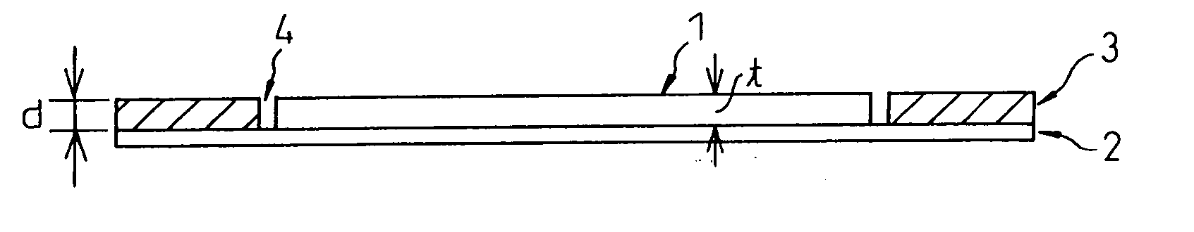
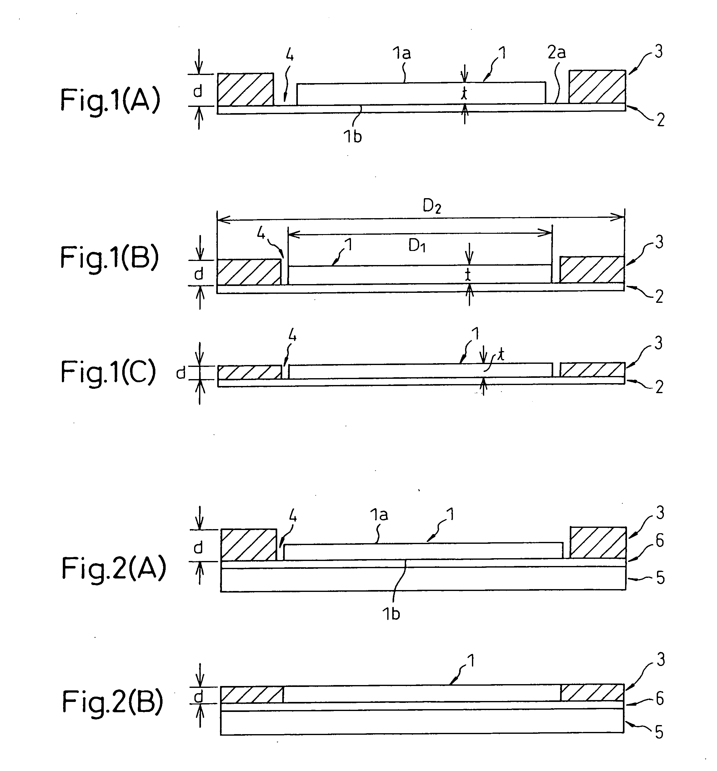
[0015] FIGS. 1(A) to 1(c) show a method for manufacturing a thin semiconductor chip of this invention. A wafer 1 is a thin disk-like configuration having a diameter (D1) of 6 inches (150 mm) and a thickness (t) of approximately 100 μm. One of the surfaces of the wafer 1 is a circuit forming surface 1a. To more easily handle the wafer 1, a tape 2 and a ring-shaped frame 3 having relatively strong base are used. One of the surfaces of the tape 2 is an adhesive surface 2a.
[0016]FIG. 1(A) shows a type A, in which a ring-shaped frame 3 having an inner diameter larger than the outer diameter of the wafer 1 is used. The upper surface of wafer in FIG. 1 is a circuit forming surface and the opposite surface 1b is adhered to the adhesive surface 2a of the tape 2. The ring-shaped frame 3 is adhered to the adhesive surface 2a of the tape 2 to encircle the outer periphery of the wafer 1. A gap 4 is defined between the outer diameter of the wafer 1 and the inner diameter of the ring-shaped frame...
second embodiment
[0019] FIGS. 2(A) and 2(B) show a method for manufacturing a thin semiconductor chip of this invention. In this embodiment, a double-face adhesive tape 6 is adhered to a rigid body 5 and the surface 1b of the wafer opposite to the circuit forming surface 1a is adhered to the double-face adhesive tape 6. In addition, a ring-shaped frame 3 is adhered to the double-face adhesive tape 6 to encircle outer the periphery of the wafer 1. The wafer 1 itself is the same as that used in the previous embodiments.
[0020]FIG. 2(A) shows a case in which the height (d) of the ring-shaped frame 3 is larger than the thickness (t) of the wafer 1 and FIG. 2(B) shows a case in which the height (d) of the ring-shaped frame 3 is substantially the same as the thickness (t) of the wafer 1.
[0021] A rigid body 5 may be a glass, particularly a silica glass, a wafer, a metal, a polymer or the other, which can be selected in relation to a method for peeling it from the double-face adhesive tape 6. The double-fac...
third embodiment
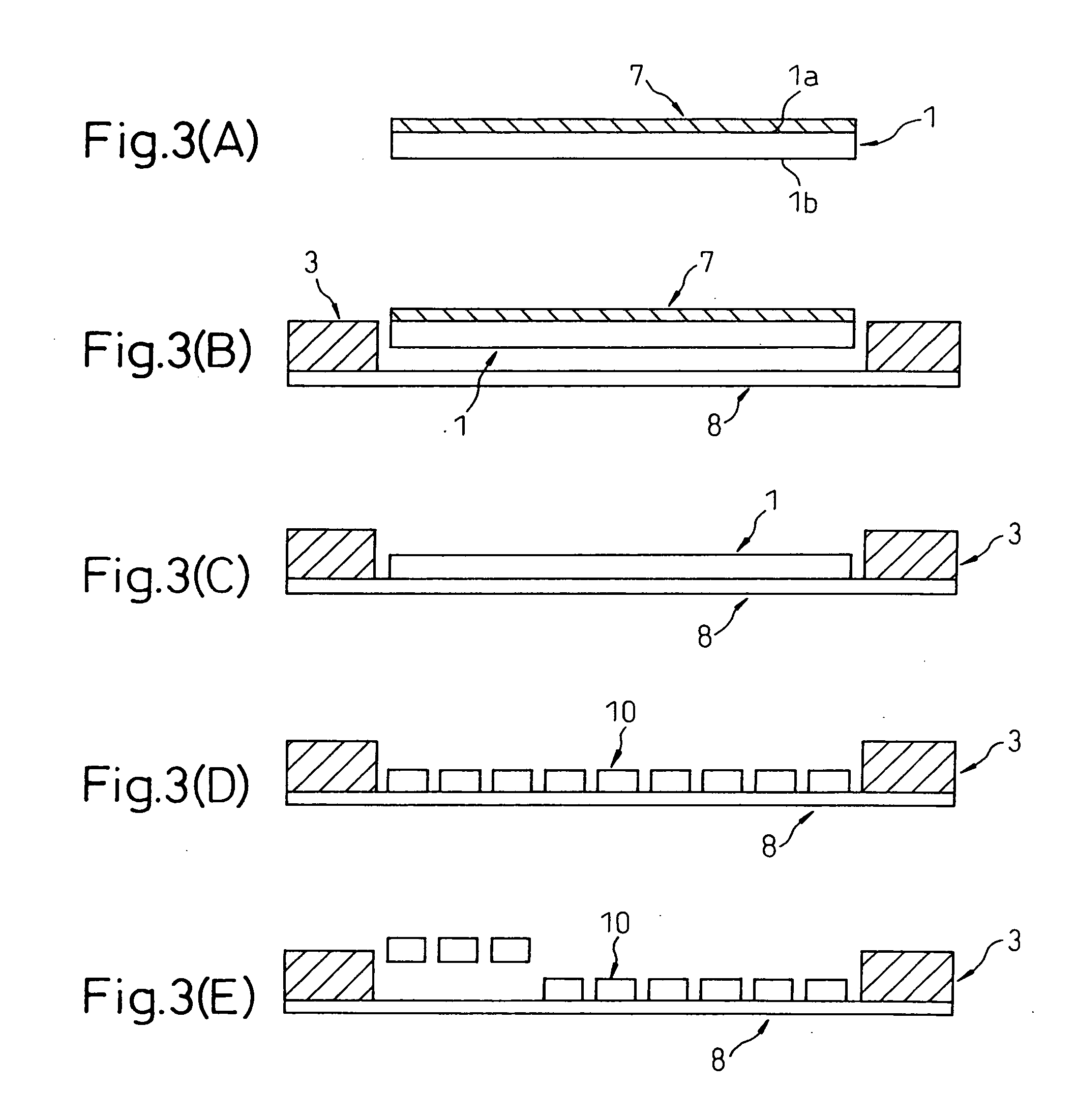
[0023] FIGS. 3(A) to 3(E) illustrate respective steps in a method for manufacturing a thin semiconductor chip of this invention. In a step (A), a protective tape 7 is adhered to a circuit forming surface 1a of the thin wafer 1.
[0024] Next, in step (B), a dicing tape 8 is adhered to a surface 1b of the thin wafer 1 opposite to the circuit forming surface 1a. The ring-shaped frame 3 is adhered to the dicing tape 8 to encircle the outer periphery of the wafer 1. Although, in general, the dicing tape 8 is usually adhered after the protective tape 7 is peeled off, in this embodiment, after the wafer 1 is held by the dicing tape 8, the protective tape 7 is peeled off. Therefore, it is advantageous that the wafer is rarely be damaged.
[0025] Next, in step (C), the protective tape 7 is peeled off. Then in step (D), the thin safer 1 is diced from the side of the circuit forming surface 1a, in such a manner that the thin wafer 1 is divided into individual pieces of semiconductor chips 10. The...
PUM
 Abstract
Description
Claims
Application Information