Method of manufacturing hybrid integrated circuit device

Active Publication Date: 2005-08-11
SEMICON COMPONENTS IND LLC
View PDF6 Cites 4 Cited by
  • Summary
  • Abstract
  • Description
  • Claims
  • Application Information

AI Technical Summary

Benefits of technology

[0020] According to the methods of manufacturing a hybrid integrated circuit device of the present invention, it is possible to flatten the side surfaces of the respective circuit boards, and thereby to equalize the outer dimensions of the circuit boards. Therefore, it is possible to perform accurate alignment by using the contour of the circuit board in the subsequent processes after separating the circuit boards.
[0021] Moreover, even when the burr is generated on the side surfaces of the circuit board in the separating step, it is possible to integrate the burr with the side surfaces of the circuit board by pressing the side sur

Problems solved by technology

However, the above-described method of manufacturing a hybrid integrated circuit device has the following problems.
Specifically, outer dimensions of the boards 106 formed by stamping may vary and it is therefore difficult to achieve accurate alignment based on the con

Method used


Image

  • Method of manufacturing hybrid integrated circuit device
  • Method of manufacturing hybrid integrated circuit device
  • Method of manufacturing hybrid integrated circuit device

Examples


Example

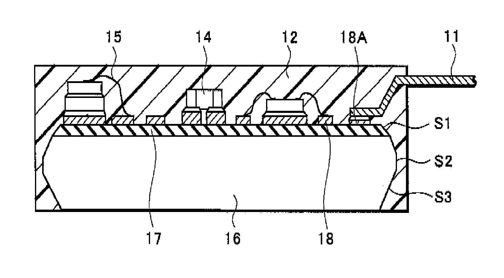
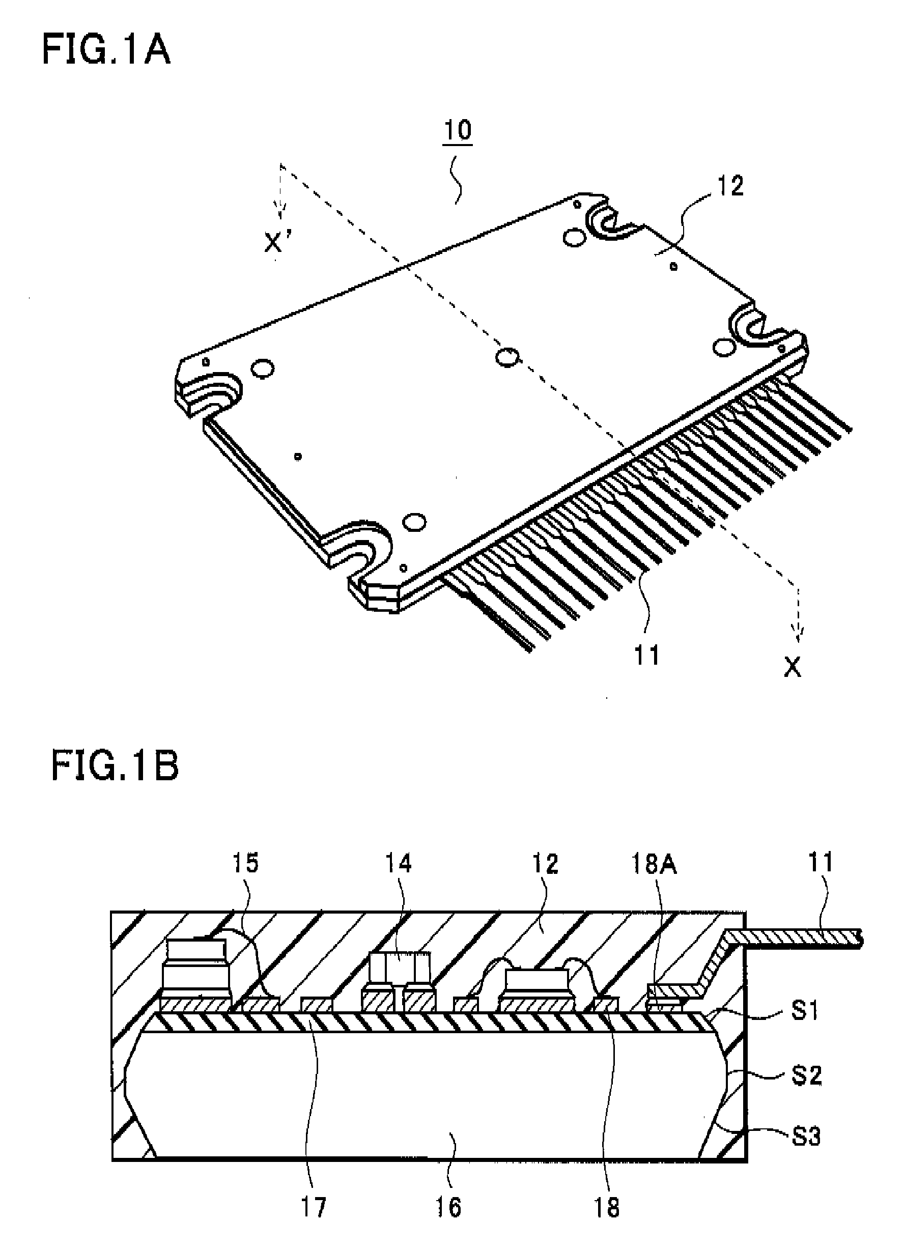
[0038] A configuration of a hybrid integrated circuit device 10 according to a preferred embodiment of the present invention will be described with reference to FIGS. 1A and 1B. FIG. 1A is a perspective view of the hybrid integrated circuit device 10, and FIG. 1B is a cross-sectional view taken along the X-X′ line in FIG. 1A.

[0039] The hybrid integrated circuit device 10 of the preferred embodiment includes a circuit board 16 having an electric circuit composed of a conductive pattern 18 and circuit elements 14 formed on a surface thereof, and sealing resin 12 for sealing the electric circuit and covering at least the surface of the circuit board 16. The respective constituents will now be described below.

[0040] The circuit board 16 is a board made of metal such as aluminum or copper. For example, when a board made of aluminum is adopted as the circuit board 16, there are two methods of insulating the circuit board 16 from the conductive pattern 18 formed on the surface thereof. T...


PUM


Abstract

A method of manufacturing a hybrid integrated circuit device includes the steps of forming a plurality of units each including a conductive pattern on a surface of a board made of metal, forming grooves along boundaries of the respective units of the board, electrically connecting circuit elements to the conductive patterns in the respective units, separating the respective circuit boards by dividing the board along the grooves, and flattening side surfaces of the circuit boards by pressing the side surfaces.

Description

CROSS-REFERENCE TO RELATED APPLICATIONS [0001] Priority is claimed to Japanese Patent Application Number JP2003-428412 filed on Dec. 24, 2003, the disclosure of which is incorporated herein by reference in its entirety. FIELD OF THE INVENTION [0002] The present invention relates to a method of manufacturing a hybrid integrated circuit device, and more specifically to a method of manufacturing a hybrid integrated circuit device including a step of dividing a board after incorporating a plurality of electric circuits on a surface thereof. DESCRIPTION OF THE RELATED ART [0003] A configuration of a conventional hybrid integrated circuit device will be described with reference to FIG. 12A and FIG. 12B (see Patent Document 1, for example). FIG. 12A is a perspective view of a hybrid integrated circuit device 100, and FIG. 12B is a cross-sectional view taken along the X-X′ line in FIG. 12A. [0004] The conventional hybrid integrated circuit device 100 has the following configuration. The hyb...

Claims


Application Information

Patent Timeline
IPC IPC(8): H01L21/301H05K1/02H01L21/48H01L21/50H01L21/56H01L21/60H01L23/12H01L23/433H01L23/498H01L25/04H01L25/16H01L25/18H05K1/05H05K3/00H05K3/28
CPCH01L21/481H01L2224/48472H01L23/4334H01L23/49861H01L24/97H01L25/165H01L2224/48091H01L2224/48227H01L2224/73265H01L2224/97H01L2924/01013H01L2924/01015H01L2924/01029H01L2924/01033H01L2924/01082H01L2924/14H01L2924/18301H01L2924/19041H01L2924/19043H01L2924/19105H05K1/056H05K3/0052H05K3/284H05K2201/09036H05K2201/0909H05K2201/1034H05K2203/0278H05K2203/302H01L21/565H01L2924/01023H01L2924/01006H01L2924/01005H01L24/48H01L2224/85H01L2924/00014H01L2224/83H01L2924/00H01L2224/451H01L2924/12042H01L2924/181H01L2224/45099H01L2224/05599H01L2924/00012H01L21/30
Inventor KANAKUBO, MASARU
Owner SEMICON COMPONENTS IND LLC
Why Eureka
Try Eureka