Adaptive clock skew in a variably loaded memory bus

a memory bus and adaptive clock technology, applied in the direction of digital transmission, generating/distributing signals, instruments, etc., can solve the problems of inability to produce a waveform with such sharp voltage transitions, the microprocessor's data storage capacity is limited, and the transfer of information between the various components of the computer system becomes more complicated

Inactive Publication Date: 2005-08-18
HEWLETT PACKARD DEV CO LP
View PDF9 Cites 7 Cited by
  • Summary
  • Abstract
  • Description
  • Claims
  • Application Information

AI Technical Summary

Benefits of technology

[0017] The selective phase lag of clock signals within a computer system may be implemented in multiple locations. In one embodiment, a phase lag circuit is disposed between the source of a clock signal and the device which uses that clock signal to read or write information onto the data bus. Disposing the clock delay circuit in this location gives this embodiment the ability to adjust the phase lag (or time delay) of only a single clock signal. A second embodiment is a computer system that has a variable path length circuit within the feedback loop of a phased locked loop (PLL) device. By selectively adjusting the length of the feedback path of the PLL, this embodiment adjusts the phase relationship of all the PLL output signals with respect to the PLL input signal. In this way, multiple clock signals can be adjusted by varying the length of the feedback path of the PLL.
[0018] Another embodiment is a computer system having both the variable length feedback path circuit in the feedback of the PLL and one or more clock delay circuits coupled to the various clocks of the system. In this way, each of the paths (the PLL feedback path and the clock circuit path) may be adjusted to provide an even more adaptive mechanism for adjusting phase lag and time delay of clock signals based on the amount of parasitic capacitance present in the system.

Problems solved by technology

However, a microprocessor is limited in its data storage capacity, and thus computer systems also have memory devices that store information for the microprocessor and other computer system components.
As computer microprocessor speeds increase, the transfer of information between the various components of the computer system becomes more complicated.
Stated another way, no physical system is capable of producing a waveform with such sharp transitions in voltage.
In a system having a bus transfer scheme operating at 133 MHz, a rise time as slow as that indicated in FIG. 2 causes significant problems in the transfer of information.
Given that most exchanges of information happen on a rising or a falling edge of the clock signal, it is apparent that a computer system having a parasitic capacitance resulting in a waveform of that of FIG. 2 would not be capable of transferring information even on the rising edges only of a 133 MHz clock, as it would take more than one complete period for the voltage to develop on the trace of the data bus.
Computer manufacturers have been somewhat successful in managing this parasitic capacitance to keep it at a level below which causes problems as the speed of data transfers have increased.
Each time the end user adds a component to the system, that user also adds parasitic capacitance, which affects the data transfer capability in the system.

Method used


Image

  • Adaptive clock skew in a variably loaded memory bus
  • Adaptive clock skew in a variably loaded memory bus
  • Adaptive clock skew in a variably loaded memory bus

Examples


Embodiment Construction

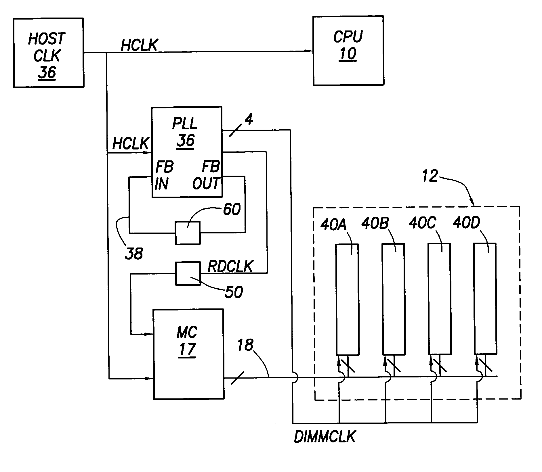
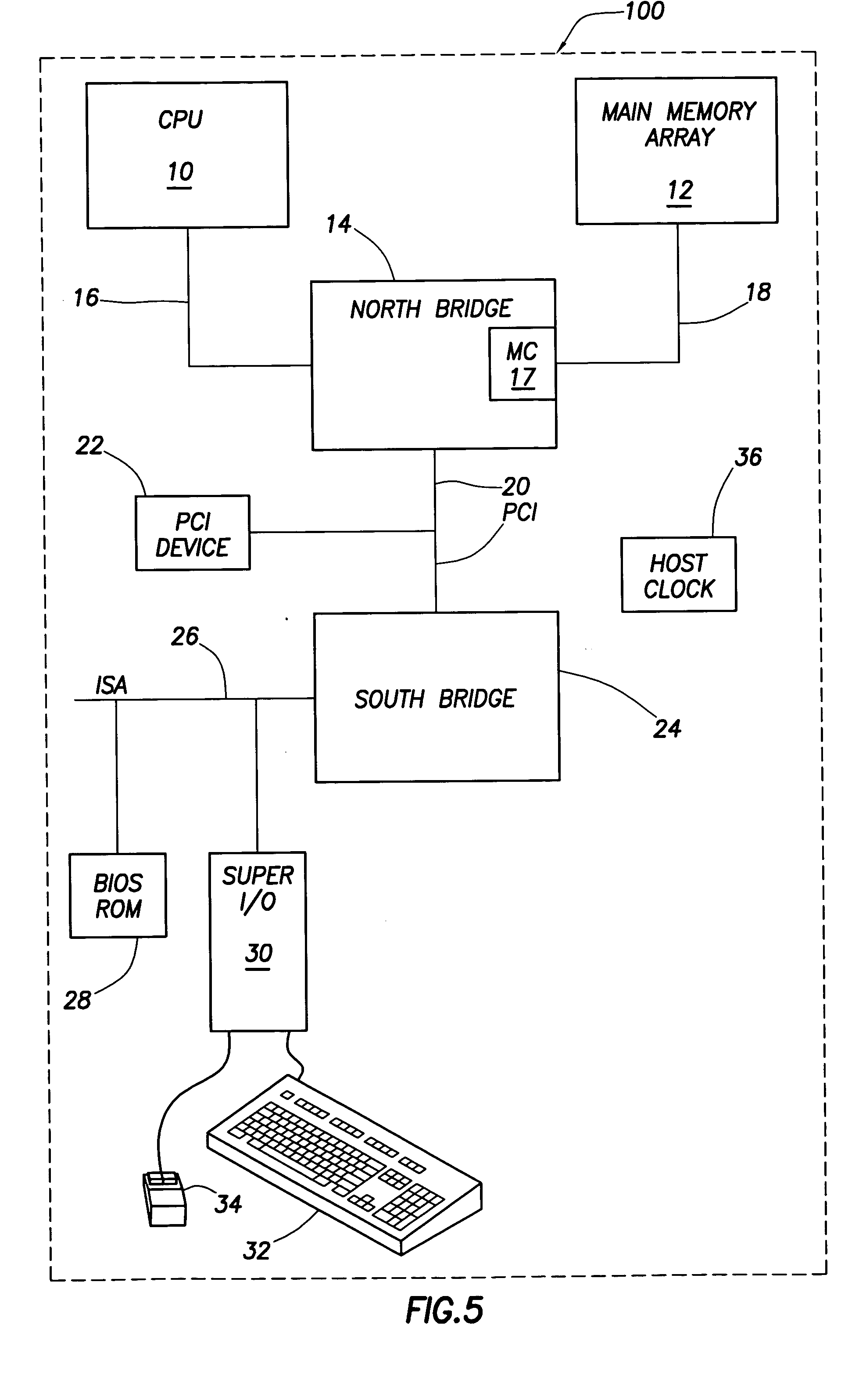
[0031] Referring now to FIG. 5, computer system 100, in accordance with the preferred embodiment, preferably comprises a processor or CPU 10 coupled to a main memory array 12 through an integrated bridge logic device 14. As depicted in FIG. 2, the bridge logic device 14 is sometimes referred to as a “North bridge,” based generally upon its location within a computer system drawing. The CPU 10 preferably couples to the bridge logic 14 via a CPU bus 16, or the bridge logic 14 may be integrated into the CPU 10. The CPU 10 preferably comprises a Pentium Pentium III® microprocessor manufactured by Intel®. It should be understood, however, that other alternative types and brands of microprocessors could be employed. Further, an embodiment of computer system 100 may include multiple processors, with each processor coupled through the CPU bus 16 to the bridge logic unit 14. To increase memory capability, and memory bus bandwidth, multiple bridge logic units 14 may be used, each coupled to i...


PUM


Abstract

The preferred embodiments of the present invention are directed to the selective phase lag and time delay of clock signals within a computer system to compensate for additional parasitic capacitance that may be added to that system because of its open architecture. More particularly, the preferred embodiments are directed to clock signal path circuits where each circuit has multiple signal paths of varying lengths. By allowing the clock signals to propagate along a particular path, phase lag or time delay is added to those clock signals. Selection of a particular path for the clock signal is made by activating electrically controlled switches which themselves are activated or deactivated by software programs that run during power-up of the computer system that determine required phase lag or time delay of those clock signals as a function of parasitic capacitance in the computer system.

Description

CROSS-REFERENCE TO RELATED APPLICATIONS [0001] This application is a divisional of application Ser. No. 09 / 904,814 filed Jul. 13, 2001, entitled “System and Method for Adaptively Adjusting Clock Skew In a Variably Loaded Memory Bus,” which application is incorporated by reference herein as if reproduced in full below.BACKGROUND [0002] The present invention relates generally to computer systems having open architecture buses. More particularly, the present invention relates to compensating for the insertion or removal of additional random access memory devices in a computer system. More particularly still, the invention relates to adjusting clock skew to compensate for the electrical characteristic changes associated with the insertion or removal of random access memory devices. [0003] Computers represent information in a binary format. That is, computers represent information in variables that have only two states, otherwise known as digital variables. In the electrical context, the...

Claims


Application Information

Patent Timeline
Patent Type & Authority Applications(United States)
IPC IPC(8): G06F1/10
CPCG06F1/10
Inventor MCBRIDE, CHRISTOPHER D.BROWNELL, PAUL V.MCJUNKIN, TIMOTHY R.
Owner HEWLETT PACKARD DEV CO LP
Why Eureka
Try Eureka