Design aid apparatus, design aid method, and computer-executable program

Inactive Publication Date: 2005-08-18
PANASONIC CORP
View PDF5 Cites 2 Cited by
  • Summary
  • Abstract
  • Description
  • Claims
  • Application Information

AI Technical Summary

Benefits of technology

[0023] According to these constructions, when a design operation of placement of objects for the multilayer wiring board is conducted in the form of division of labor with support of the first and second aid units, the boundary design information relating to both the first and second portions is managed and displayed by both the first and second aid units. This enables each aid unit to easily check the changes made to the boundary design information by the other aid unit.
[0051] According to this method, the same effects as the above design information conversion apparatus can be achieved.

Problems solved by technology

This method, however, has the following problem.
If the flexibility is excessively high, an enormous amount of time and effort is needed for a design operation even with the help of the above design aid apparatus.
Though not able to achieve an optimum packaging density, this design method treats fewer layers in each partial design process, thereby limiting the flexibility in placement of components.
In the absence of a design aid apparatus for totally and effectively aiding in design of a multilayer wiring board according to the above design method, however, the following problem arises.
In view of a significant increase in size of circuitry which is subjected to design in recent years, this method is no longer practical.
According to this method, however, it is difficult to perform each partial design process in the form of division of labor, so that the effect of shortening the design time lessens.

Method used


Image

  • Design aid apparatus, design aid method, and computer-executable program
  • Design aid apparatus, design aid method, and computer-executable program
  • Design aid apparatus, design aid method, and computer-executable program

Examples


first embodiment

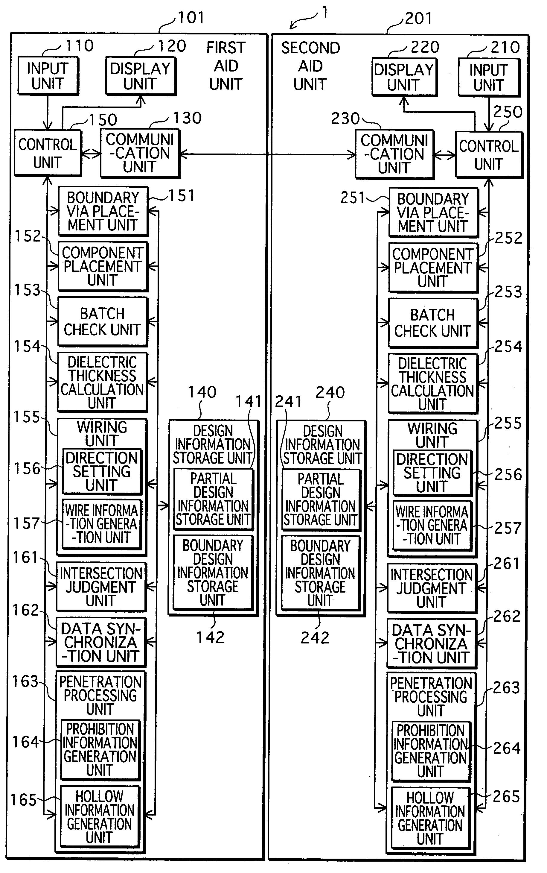
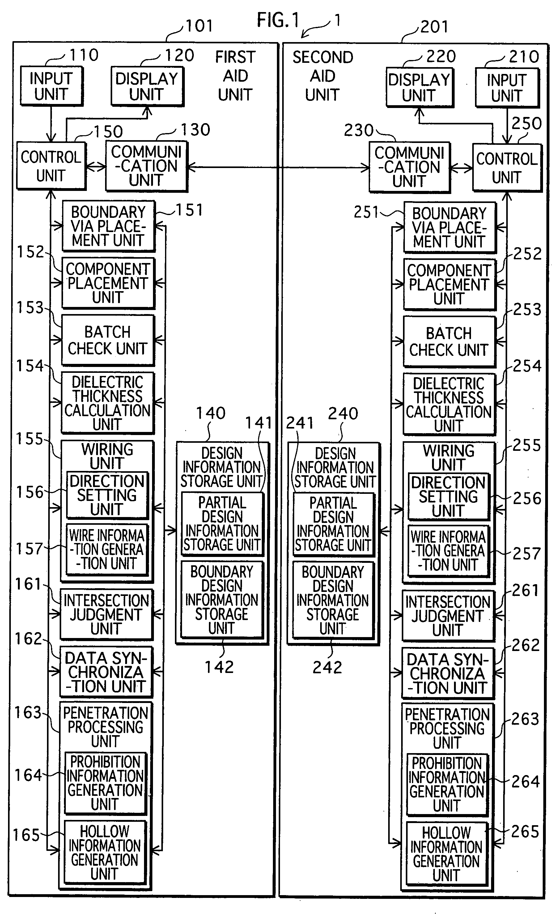
[0098] A design aid apparatus to which a first embodiment of the present invention relates aids in design of placement of objects to a multilayer wiring board which is formed by laminating a plurality of dielectrics, separately for each board portion made up of a set of dielectrics.

[0099] The plurality of dielectrics include at least one specific dielectric in which components can be embedded. This being so, the design aid apparatus has a first aid unit corresponding to a first board portion which is made up of a set of dielectrics adjacent to one side of the specific dielectric, and a second aid unit corresponding to a second board portion which is made up of a set of dielectrics adjacent to the other side of the specific dielectric.

[0100] Design of each board portion is conducted on the assumption that the board portion itself is one multilayer wiring board. In view of this, the first and second board portions are hereafter also referred to as partial boards which are treated as...

second embodiment

[0319] The following describes a design information conversion apparatus to which a second embodiment of the present invention relates, with reference to drawings. The design information conversion apparatus converts partial design information and boundary design information described in the first embodiment to total design information about an entire multilayer wiring board, and converts the total design information back to the partial design information and the boundary design information.

[0320] One multilayer wiring board is designed in the state of being separated into a plurality of partial boards, under the aid of the design aid apparatus of the first embodiment. After this, the multilayer wiring board is manufactured as a single board. Accordingly, partial design information and boundary design information are suitably used in the design process, whereas total design information is suitably used the manufacturing process. The design information conversion apparatus provides ...


PUM


Abstract

A multilayer wiring board formed by laminating a plurality of dielectrics including a specific dielectric capable of embedding components therein is separated into first and second portions that are respectively made up of sets of dielectrics on opposite sides of the specific dielectric. A first aid unit stores design information about placement of objects to the first portion, and manages and displays the design information according to a user command to aid in design of the first portion. A second aid unit stores design information about placement of objects to the second portion, and manages and displays the design information according to a user command to aid in design of the second portion. Further, the first and second aid units each store design information about placement of boundary objects which extend to both the first and second portions, and cooperatively manage the design information and each display it.

Description

[0001] This application is based on an application No. 2004-040384 filed in Japan, the contents of which are hereby incorporated by reference. BACKGROUND OF THE INVENTION [0002] 1. Field of the Invention [0003] The present invention relates to a design aid apparatus for aiding in design of placement of objects for a multilayer wiring board. The present invention in particular relates to techniques of aiding in separately designing different board portions which are set in a lamination direction of the multilayer wiring board. [0004] 2. Related Art [0005] Conventionally, electronic devices which need to be made smaller in size are often implemented using multilayer wiring boards. [0006] An advanced manufacturing technique in recent years makes it possible to produce multilayer wiring boards in which tiny components such as bare chip semiconductors are embedded (for example, see the news release article dated Sep. 9, 2002 by Matsushita Electric Industrial Co., Ltd. “Development of New...

Claims


Application Information

Patent Timeline
IPC IPC(8): G06F17/50H05K3/00
CPCG06F17/5068G06F30/39
Inventor IKEDA, HIROSHINAKAYAMA, TAKESHI
Owner PANASONIC CORP
Why Eureka
Try Eureka