
Method for optimization of logic circuits for routability

a logic circuit and optimization method technology, applied in the field of circuits, can solve the problems of design closure increasing correspondingly at a geometric rate, routability of the circuit, and impossible to do

Inactive Publication Date: 2005-08-18
GOOGLE LLC
View PDF8 Cites 15 Cited by
  • Summary
  • Abstract
  • Description
  • Claims
  • Application Information

AI Technical Summary

Problems solved by technology

As the size of the VLSI chip grows, the problem of design closure increases correspondingly at a geometric rate.
A key design parameter that affects design closure significantly is routability of the circuit.
In some cases, this may be impossible to do; that is, the chip is said to be unroutable.
Routability (or wiring congestion) affects the performance, noise sensitivity, yield, area, and power of the design.
While the technology independent synthesis optimizations attempt to measure the size and speed of the circuit, no metrics exist to determine where the literals will be placed or how many wiring paths will want to follow similar routes, which correlates strongly with the routability of the design.
While delay receives attention early in the design process, if all of the connections between the design components cannot be made, the design cannot be implemented.
Poor routability of the design also creates longer wires in the design, causing a degradation in timing.
If the inability to route the design or the inability to meet timing due to poor routability is discovered only during the physical design process, a designer must return to the technology independent logic synthesis phase to alter the way the design was optimized.
However, since those optimizations have no concept of a routability metric, it is difficult to direct those optimizations toward a criteria that cannot be measured.
Therefore, existing optimizations and transformations in the logic synthesis stage, which are primarily targeted towards timing and area, generally do not consider their impact on routability.
Optimizations in this step use a literal count as a metric for optimization, and, therefore, do not adequately capture the intrinsic entanglement of the circuit.
In this scenario, decisions made in the early stages of design flow become binding constraints on later stages.
Such serialization potentially gives less optimal designs than a process that simultaneously considers all design aspects.
This is unavoidable, however, due to the practical infeasibility of concurrent optimization of all design parameters, and is deemed acceptable as long as the constraints that are fed forward by one step to the next can be met.
The process breaks down, however, when these constraints become unsatisfiable (e.g., the chip becomes unroutable, and falls short of the expected yield).
Techniques which optimize both the logical and physical characteristics are referred to as physical synthesis Although, there is work in the area of physical synthesis that combines later stages of logic synthesis with placement, the early stages of logic synthesis are not adequately integrated with placement.
Although the locations of chip / partition Inputs / Outputs are typically available, assumptions about locations for pins surrounding the small region consisting of a few gates in which local optimizations (e.g., factorizations) are being performed is generally difficult to preserve during full chip placement.
Furthermore, statistical interconnect prediction methods (e.g., Rent's rule) do not distinguish between two networks which have the same number of connections.
Therefore, they are unsuitable as predictors for routability optimization during technology independent synthesis.

Method used


Image

  • Method for optimization of logic circuits for routability
  • Method for optimization of logic circuits for routability
  • Method for optimization of logic circuits for routability

Examples


Embodiment Construction

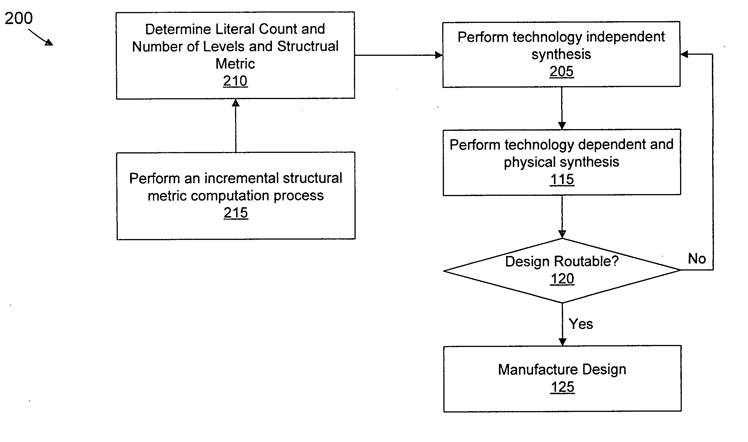
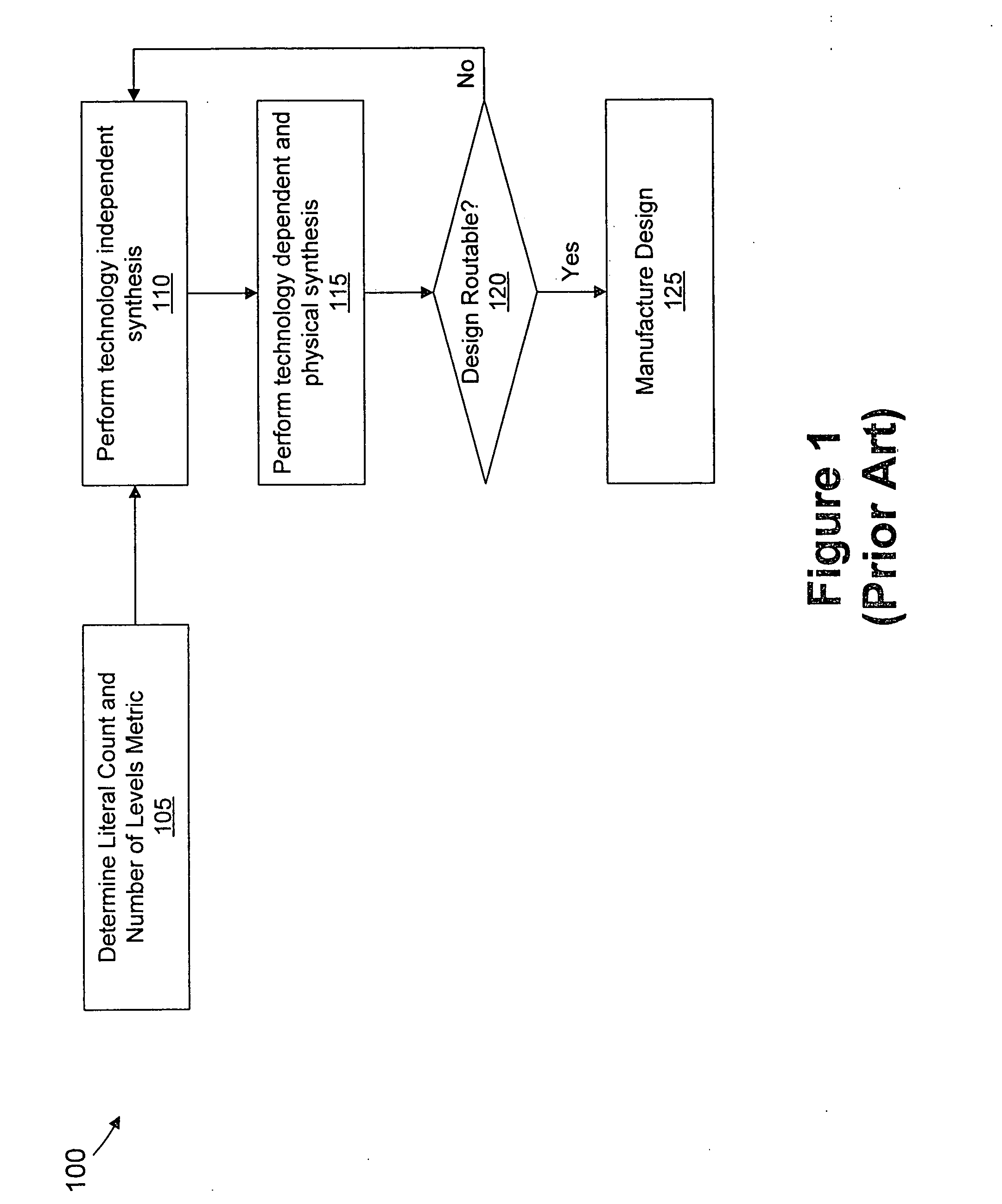
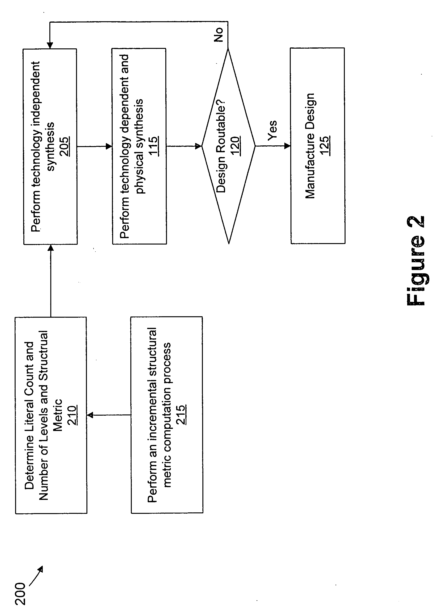
[0037] Illustrative embodiments of the invention are described below. In the interest of clarity, not all features of an actual implementation are described in this specification. It will of course be appreciated that in the development of any such actual embodiment, numerous implementation-specific decisions must be made to achieve the developers' specific goals, such as compliance with system-related and business-related constraints, which will vary from one implementation to another. Moreover, it will be appreciated that such a development effort might be complex and time-consuming, but would nevertheless be a routine undertaking for those of ordinary skill in the art having the benefit of this disclosure.

[0038] While the invention is susceptible to various modifications and alternative forms, specific embodiments thereof have been shown by way of example in the drawings and are herein described in detail. It should be understood, however, that the description herein of specific...


PUM


Abstract

Routability (or wiring congestion) in a VLSI chip is becoming increasingly important as chip complexity increases. Congestion has a significant impact on performance, yield, and chip area. The present invention targets the optimization of congestion early in technology independent synthesis prior to physical design. Instead of attempting to optimize the logic structure as well as the spatial placement of a circuit, we pose a more modest goal limiting such optimization to the scope of logic synthesis. That is, we propose an aggressive optimization approach that is cognizant of circuit structure during technology independent synthesis and produces more predictable implementations which give better routability and yield.

Description

BACKGROUND OF THE INVENTION [0001]1. Field of the Invention [0002] The present invention relates to circuits and, more particularly, to electronic circuit design. [0003]2. Description of the Related Art [0004] A major goal in the design of Very Large Scale Integration (“VLSI”) chips and other integrated circuits is to combine logic synthesis methods with physical design optimization methods to meet timing, area, and other design objectives of the chip. Physical design optimization methods include methods for placement and methods for routing. Logic synthesis methods determine the type and connectivity of circuits used to implement the functionality of the chip. Placement methods assign and alter the physical locations of the circuits on the chip. Routing methods modify the physical path and wire type of the connections between the circuits. [0005] As the size of the VLSI chip grows, the problem of design closure increases correspondingly at a geometric rate. Design closure is the pr...

Claims


Application Information

Patent Timeline
IPC IPC(8): G06F17/50
CPCG06F17/505G06F30/327
Inventor DOUGHERTY, WILLIAM E. JR.KRAVETS, VICTORKUDVA, PRABHAKAR N.SULLIVAN, ANDREW J.
Owner GOOGLE LLC
Learn More