Phase change memory cell and method of its manufacture

a memory cell and phase change technology, applied in the direction of bulk negative resistance effect devices, electrical equipment, semiconductor devices, etc., can solve the problems of limit the voltage that can be applied by a mosfet to a chalcogenide memory cell before mosfet breakdown

Inactive Publication Date: 2005-08-25
TAIWAN SEMICON MFG CO LTD
View PDF8 Cites 32 Cited by
  • Summary
  • Abstract
  • Description
  • Claims
  • Application Information

AI Technical Summary

Problems solved by technology

MOSFETs are not optimum switch elements for phase change memories, because they have been reduced in size (reduced channel length and oxide thickness).
Accordingly, although current densities through MOSFETs have risen, there is a limit to the voltage that can be applied by a MOSFET to a chalcogenide memory cell before MOSFET breakdown occurs.

Method used


Image

  • Phase change memory cell and method of its manufacture
  • Phase change memory cell and method of its manufacture
  • Phase change memory cell and method of its manufacture

Examples


Embodiment Construction

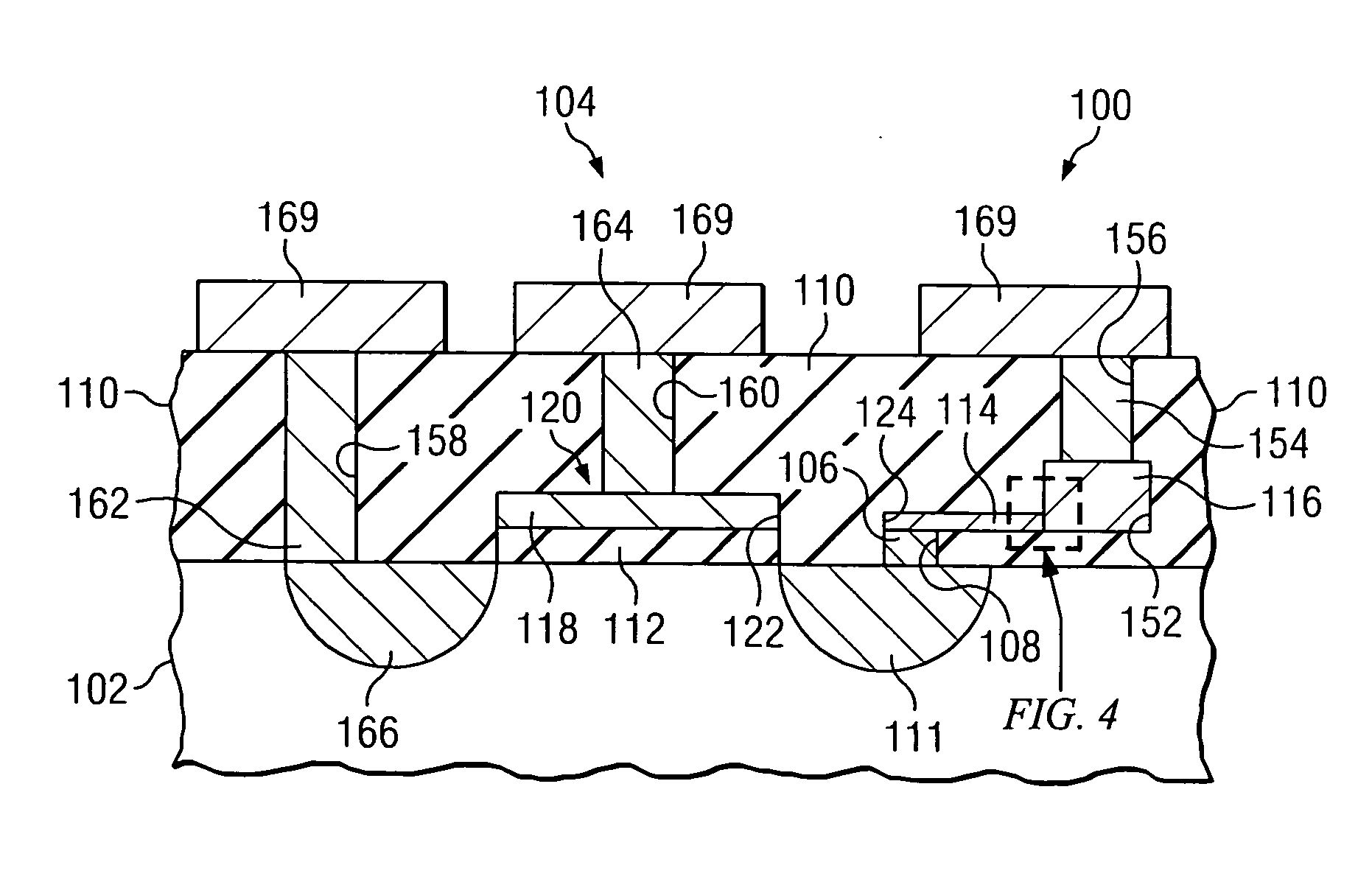
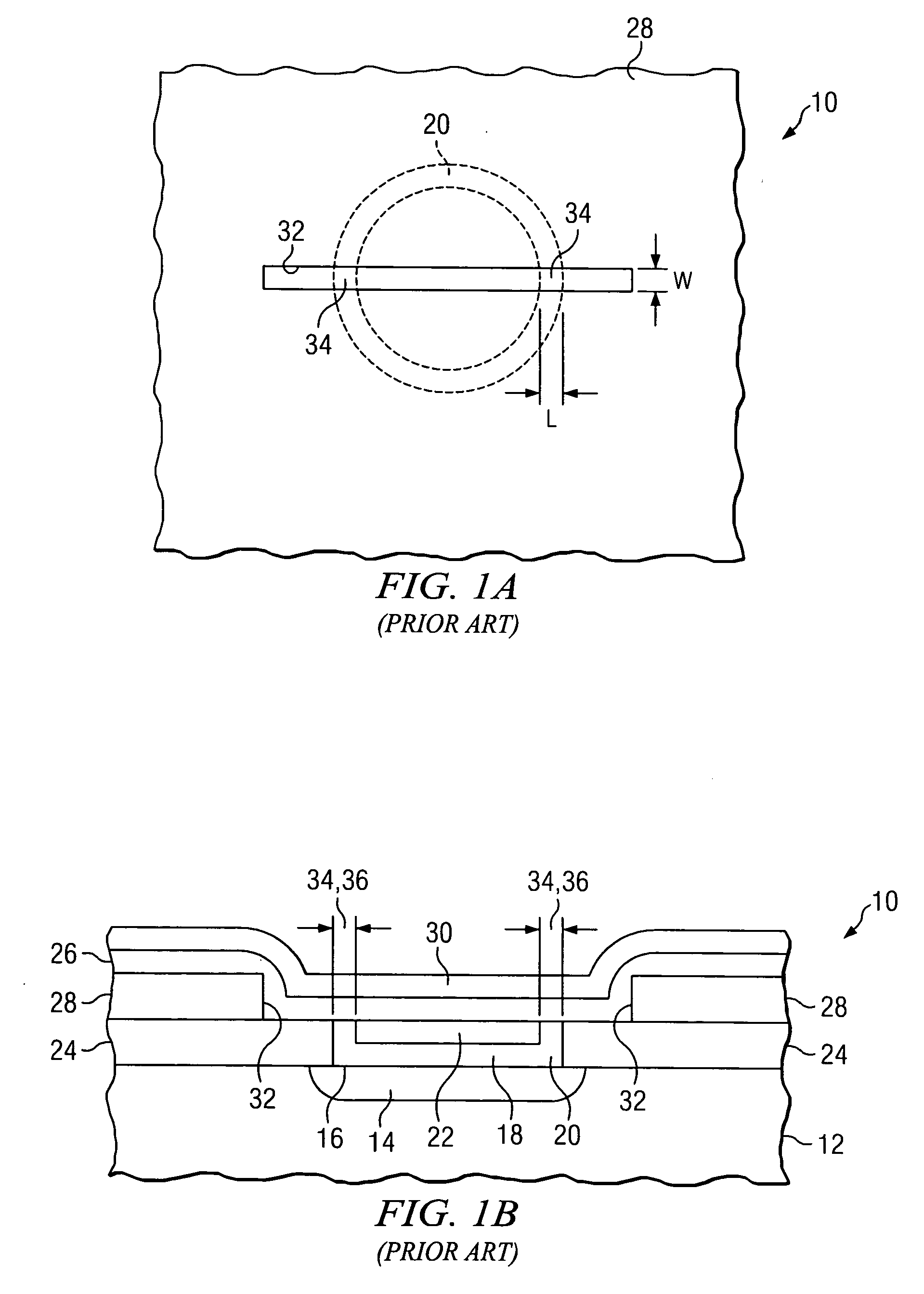
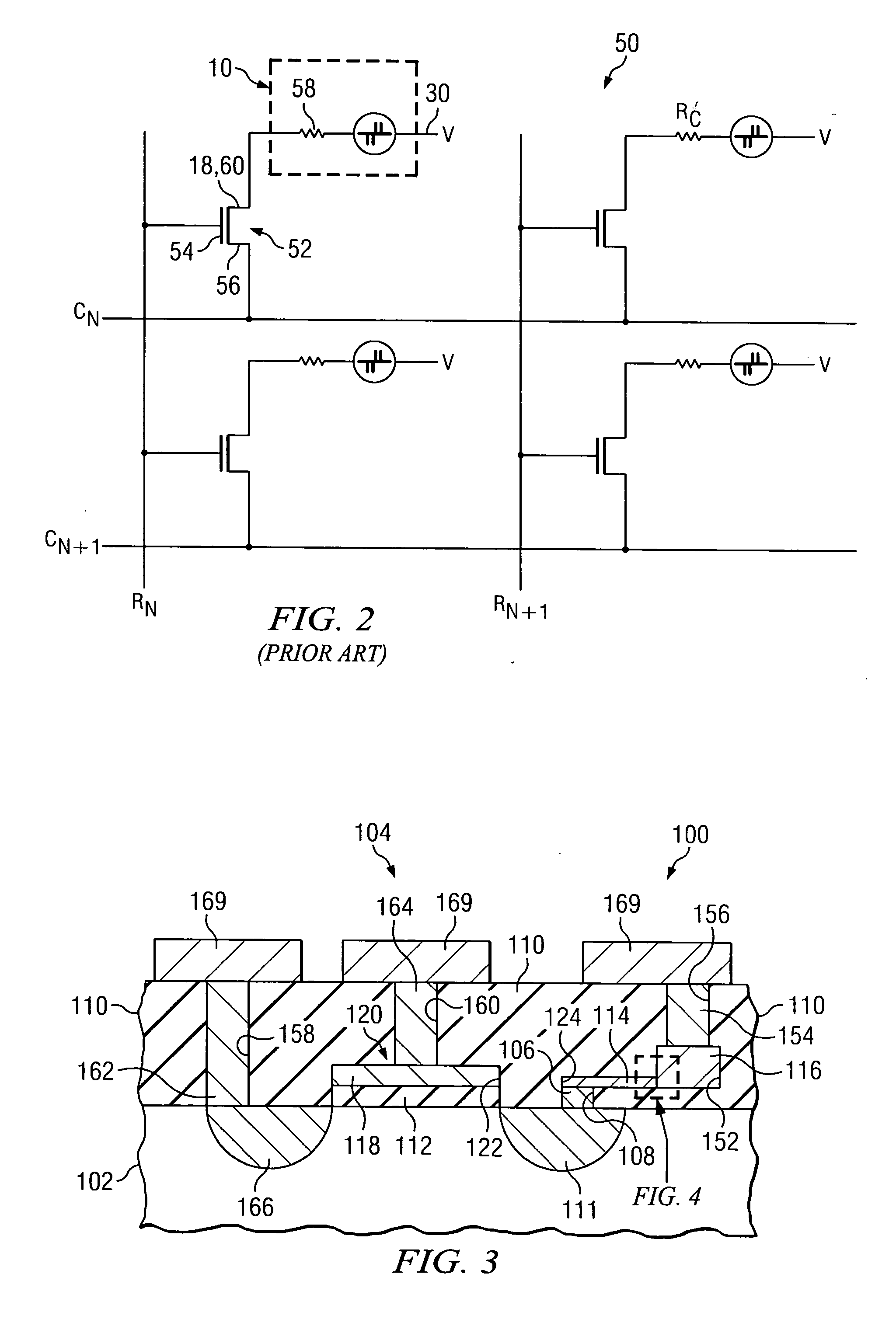
[0025] The making and using of the presently preferred embodiments are discussed in detail below. It should be appreciated, however, that the present invention provides many applicable inventive concepts that can be embodied in a wide variety of specific contexts. The specific embodiments discussed are merely illustrative of specific ways to make and use the invention, and do not limit the scope of the invention.

[0026] The product aspects of the present invention relate to an improved phase change memory cell. Preferably, the memory cell is fabricated by integrated circuit techniques and is associated with a transistor, such as a MOSFET, both being on the same substrate. The term “memory cell” refers herein to the memory cell itself and to the memory unit associated with a transistor or other switch-like device. The method aspects of the present invention relate to a method of fabricating the improved phase change memory cell. Preferred embodiments of these aspects will be discusse...


PUM


Abstract

A phase change memory cell includes a resistive heating element for a phase change body that can expeditiously and efficiently heat a portion of the body with the voltage and current usable with MOSFETs. This is achieved through minimizing the area of an interface between a conductive layer and the body by permitting photolithographic techniques to define one dimension of the interface and thin film deposition techniques to define the other dimension.

Description

TECHNICAL FIELD [0001] The present invention relates to a phase change memory cell and to the method of its manufacture. More specifically, the present invention relates to a memory cell that includes, first, a material capable of having two different temperature-dependent states and, second, facilities for efficiently and expeditiously causing the material to reside in one or the other of those states. The present invention also relates to a method of manufacturing such a memory cell. BACKGROUND [0002] Phase change memories are known. See U.S. Pat. No. 6,512,241, issued Jan. 28, 2003 to Lai (“'241” patent) and US Published Patent Application 20030122156 by Maimon, published Jul. 2, 2003 (“'156 application”), the latter containing an extensive list of prior art phase change patents. [0003] Various materials may reside in two or more different states. Two-state devices are favored for digital memories for obvious reasons. Many of these materials exhibit an amorphous state and a cryst...

Claims


Application Information

Patent Timeline
Patent Type & Authority Applications(United States)
IPC IPC(8): H01L27/24H01L45/00H01L47/00
CPCH01L27/2436H01L45/06H01L45/122H01L45/1683H01L45/144H01L45/148H01L45/126H10B63/30H10N70/231H10N70/821H10N70/8413H10N70/8828H10N70/884H10N70/066
Inventor LAI, LI-SHYUETANG, DENNY DUAN-IEELIN, WEN-CHIN
Owner TAIWAN SEMICON MFG CO LTD
Why Eureka
Try Eureka