Seal ring design without stop layer punch through during via etch

a technology of stop layer and sealing ring, which is applied in the direction of semiconductor devices, semiconductor/solid-state device details, electrical devices, etc., can solve the problems of affecting the surface cleaning process, affecting the appearance of the applied etch stop layer, etc., and achieves the effect of preventing the damage of the etch stop layer

Inactive Publication Date: 2005-08-25
TAIWAN SEMICON MFG CO LTD
View PDF6 Cites 4 Cited by
  • Summary
  • Abstract
  • Description
  • Claims
  • Application Information

AI Technical Summary

Benefits of technology

[0016] A principle objective of the invention is to create a seal ring around the perimeter of a substrate such that problems of etch stop layer damage is prevented while simultaneously creating dissimilar features such as seal ring vias having dissimilar Critical Dimensions of the seal ring.

Problems solved by technology

These two features of trench and vias are simultaneously etched, a process that may result in damage to the applied etch stop layer in view of and caused by the different Critical Dimensions of these two elements.
This exposure of the surface of layer 16 causes arcing and the introduction of copper sputtered polymers into the processing environment, which in turn makes the process of surface clean considerably more difficult.

Method used


Image

  • Seal ring design without stop layer punch through during via etch
  • Seal ring design without stop layer punch through during via etch
  • Seal ring design without stop layer punch through during via etch

Examples


Embodiment Construction

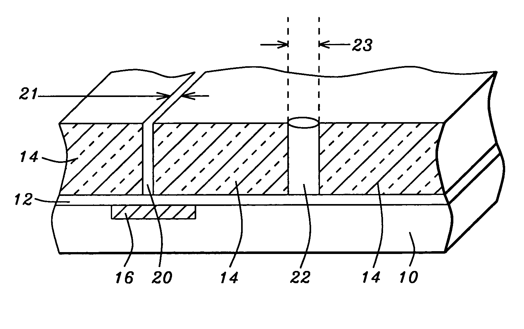
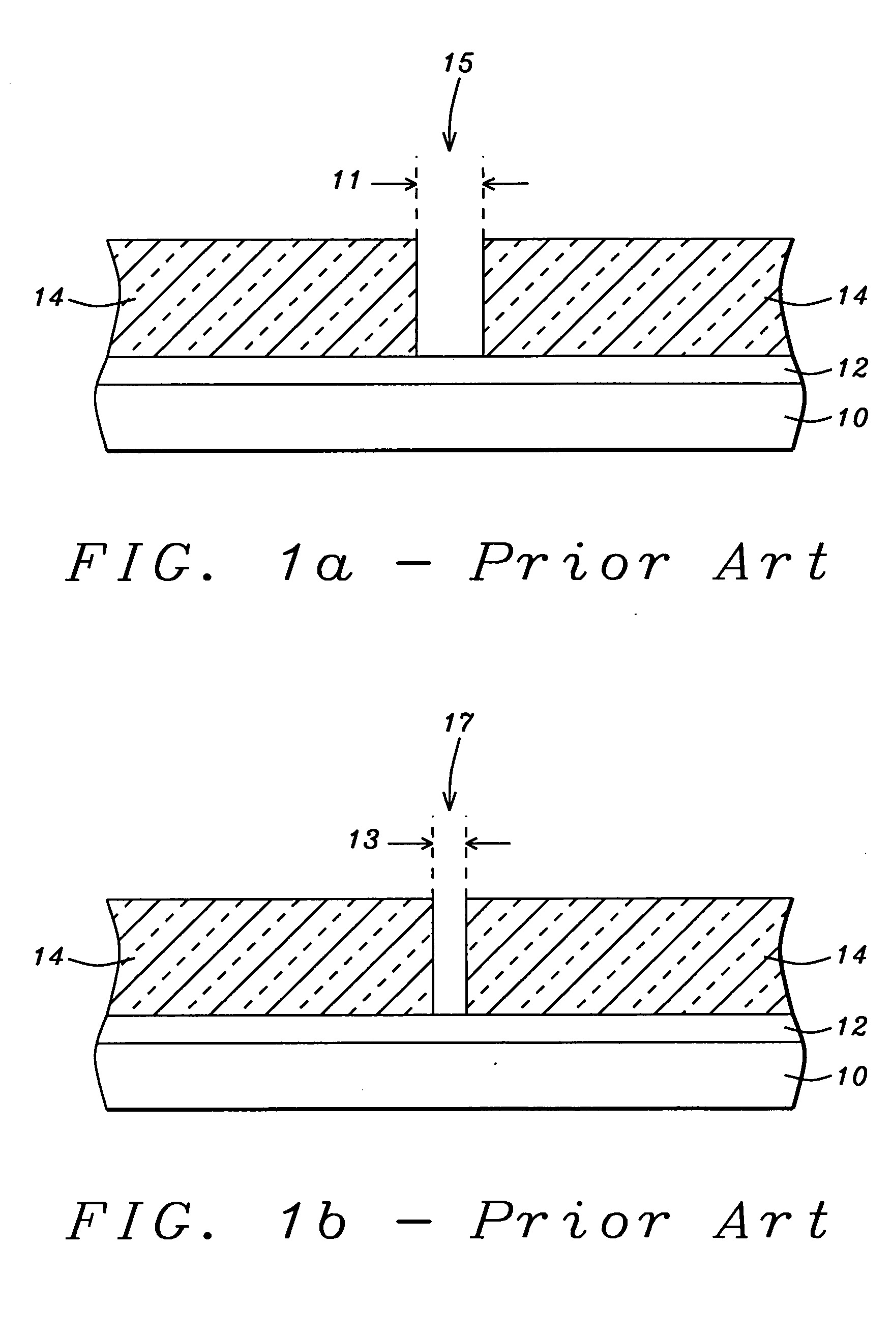
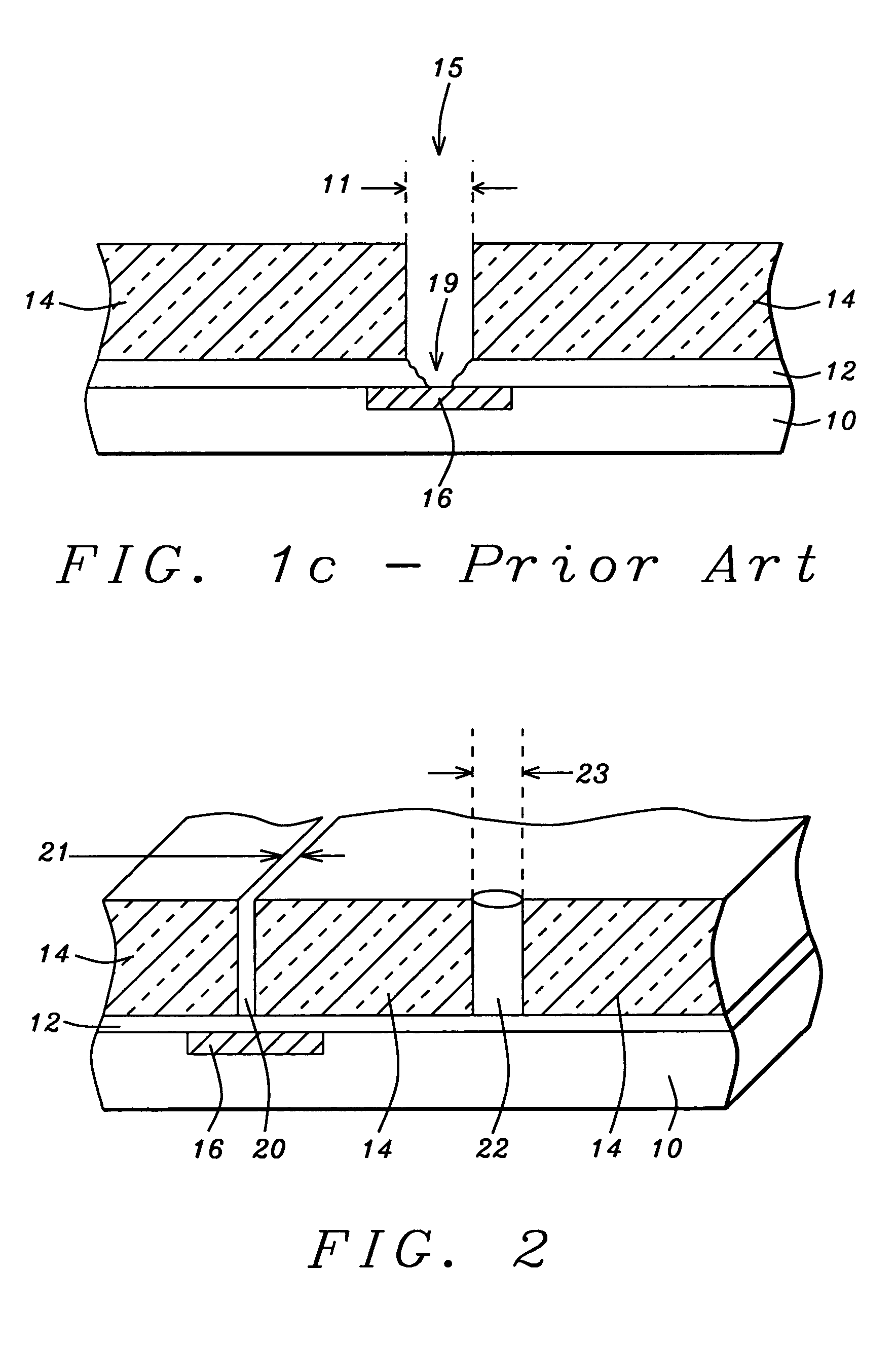
[0022] Prior Art has addressed concerns of punch through of an etch stop layer by selecting the Critical Diameter (CD) of a seal via as being smaller than the CD of a seal ring. This requires selecting the surface area that is being etched such that the etch of the seal ring and the seal via holes completes at about the same time. The invention does not follow this approach. The invention is not based on selecting the surface area of the areas that are concurrently being etched but selects the width of the seal ring and the diameter of the seal vias as the controlling parameters that enable the concurrent completion of the seal ring and the seal vias.

[0023] The invention addresses the creation of a seal ring, whereby the seal ring comprises a trench and therewith associated seal ring vias. These two features of trench and vias are simultaneously etched, a process that may result in damage to the applied etch stop layer in view of and caused by the different Critical Dimensions of t...


PUM


Abstract

In accordance with the objective of the invention a new method is provided for the creation of a seal ring having dissimilar elements. The Critical Dimensions of the seal ring are selected with respect to the CD of other device features, such a seal vias, such that the difference in etch sensitivity between the created seal ring and the via holes is removed. All etch of the simultaneously etched features is completed at the same time, avoiding punch through of an underlying layer of etch stop material.

Description

BACKGROUND OF THE INVENTION [0001] (1) Field of the Invention [0002] The invention relates to the fabrication of integrated circuit devices, and more particularly, to a method of designing a seal ring. [0003] (2) Description of the Prior Art [0004] The creation of semiconductor devices comprises numerous complex and mutually cooperative steps of semiconductor processing during which a large variety of materials and techniques are used. Processing of semiconductor devices is performed in a serial processing stream, which implies that each of the steps of the sequential processing must be essentially error free so as to avoid accumulative errors and the severe negative yield impact that would result therefrom. [0005] This latter requirement implies that semiconductor materials are created where they are required to be created, strictly controlling the occurrence of such materials in any other than the required design configuration. For instance, the accumulation of undesired matter in...

Claims


Application Information

Patent Timeline
Patent Type & Authority Applications(United States)
IPC IPC(8): H01L23/48H01L23/58
CPCH01L23/585H01L2924/0002H01L2924/00
Inventor SHIH, HSIN-CHINGLIN, KANG-CHENGCHEN, CHAO-CHENGTAO, HUN-JAN
Owner TAIWAN SEMICON MFG CO LTD
Why Eureka
Try Eureka