Dynamic random access memory having at least two buffer registers and method for controlling such a memory

a random access memory and buffer register technology, applied in the field of memory, can solve the problems of slow access, limited and narrower than that of static memories, and achieve the effect of increasing bandwidth

Active Publication Date: 2005-08-25
STMICROELECTRONICS SRL
View PDF11 Cites 10 Cited by
  • Summary
  • Abstract
  • Description
  • Claims
  • Application Information

AI Technical Summary

Benefits of technology

[0014] One embodiment of the present invention is a new structure of a dynamic memory that makes possible to further increase the bandwidth compared to known structures.

Problems solved by technology

On the other hand, they need periodic cooling and, moreover, they are much slower to access than static memories.
Although using buffer memories makes it possible to significantly increase the bandwidth of dynamic memories, it is still limited and much narrower than that of static memories.
This constitutes a first technical issue.
This constitutes a second technical issue.
Lastly, improving the reliability of dynamic memories is another problem that is added to the preceding ones.
These processes are very expensive to implement for it is necessary to carry out package and temperature tests after burn-in for the principal defects (carrying time) are visible only with high temperature; however, the carriers of some packages (and not packages themselves) deteriorate when heated, which requires to frequently change the card used for this test.

Method used


Image

  • Dynamic random access memory having at least two buffer registers and method for controlling such a memory
  • Dynamic random access memory having at least two buffer registers and method for controlling such a memory
  • Dynamic random access memory having at least two buffer registers and method for controlling such a memory

Examples


second embodiment

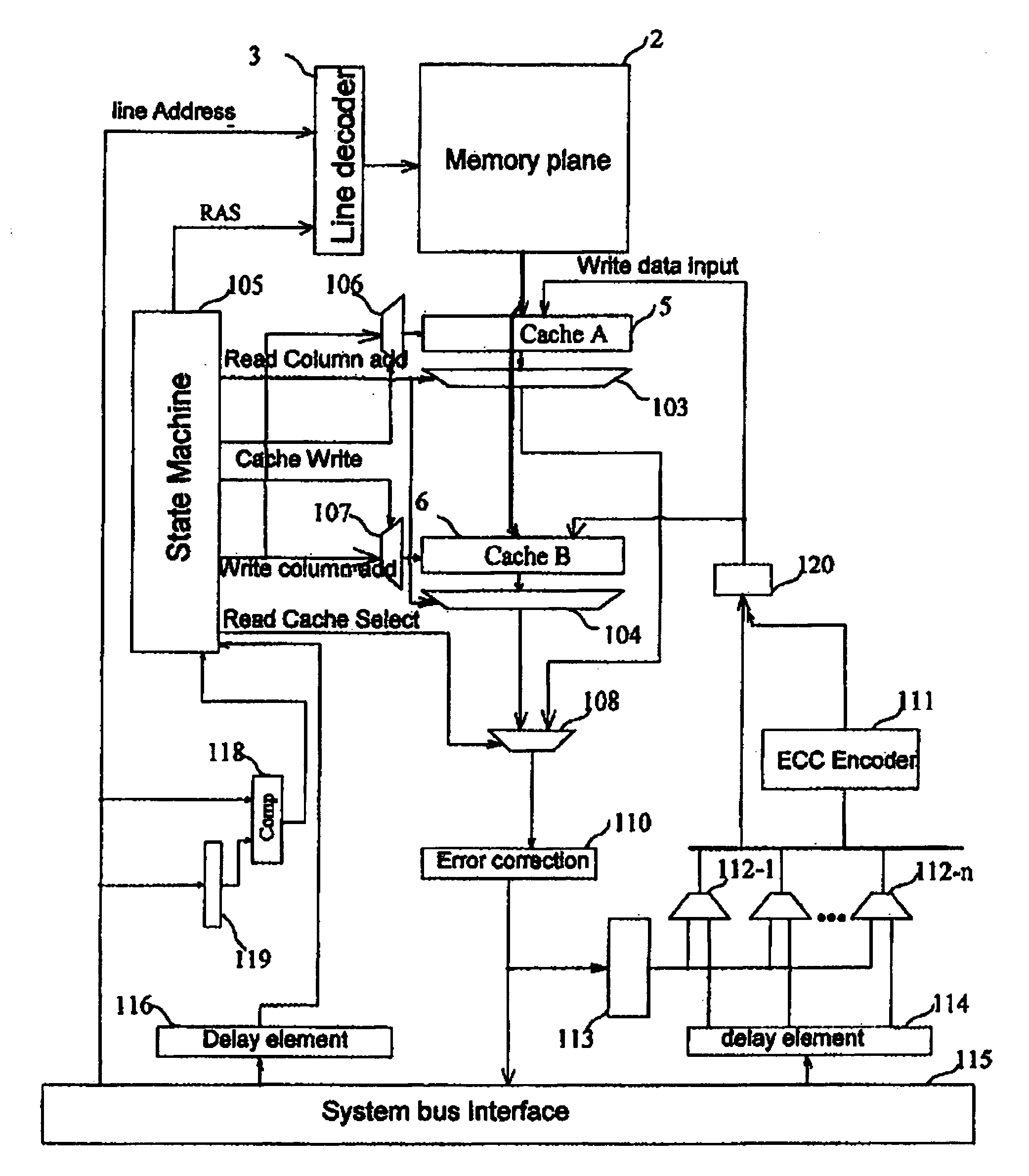
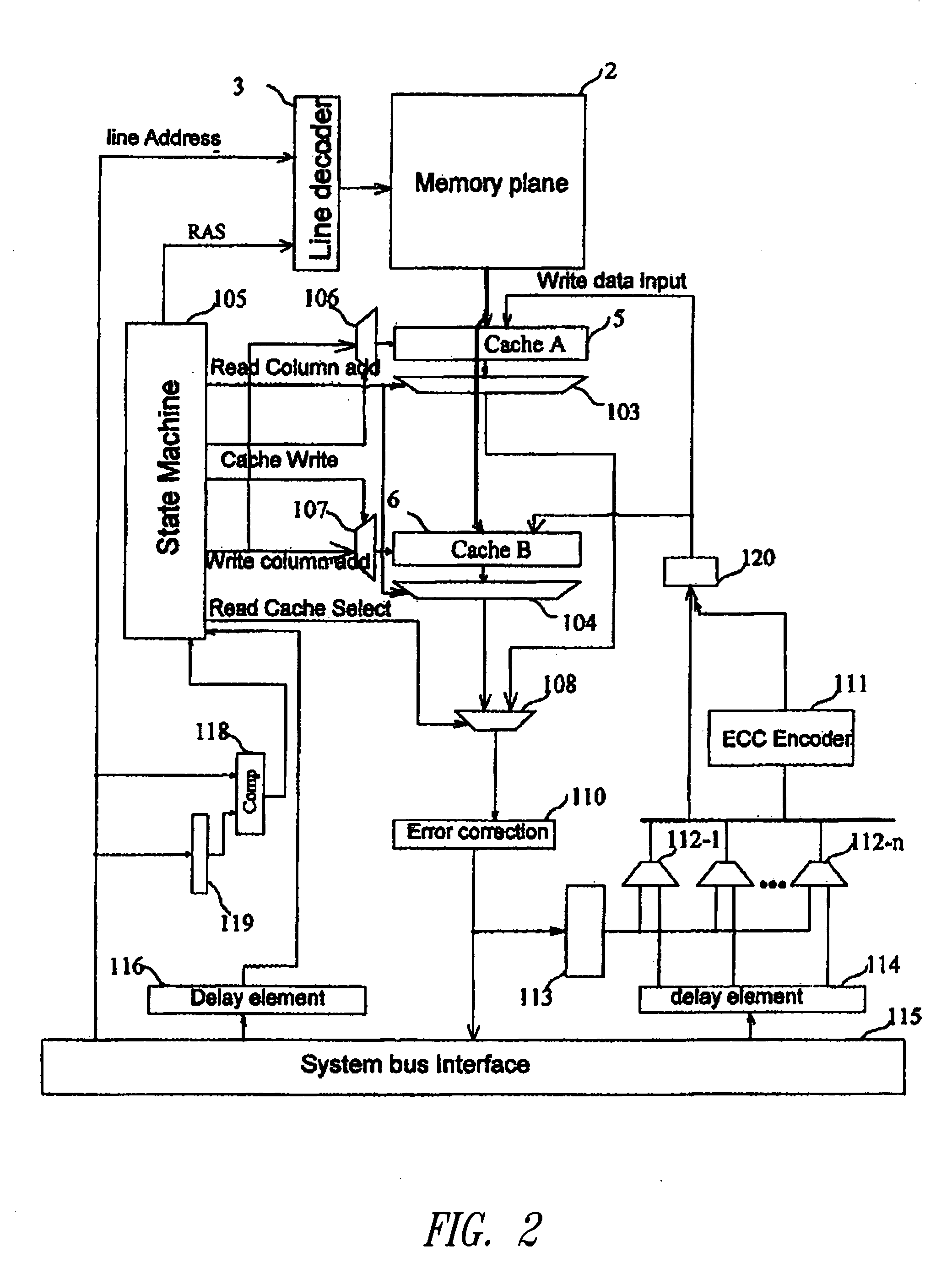
[0067] In this second embodiment, there is a set of master flip-flops—440-0 to 440-15—which are common to bits of the same row for all the words of one page.

[0068] The set of master flip-flops 440-0 to 440-15 then constitutes an input register—represented by element 120 on FIG. 2—having the width of a word group (i.e., 128 bits) and composed of simple flip-flops. The group formed by this 1-word register and one of the buffer registers then behaves as if the buffer register were composed of master-slave flip-flops, the master flip-flop 322 being in the input register and the slave flip-flop 321 in the buffer register. This solution has the advantage of reducing the occupied silicon surface.

third embodiment

[0069]FIG. 3C finally illustrates the buffer registers comprised of blocks 510-i (i varying from 0 to 7) comprising a single flip-flop 511-i-j (for example flip-flop 511-7-15), at the input of which (in register 120 of FIG. 2) is associated a master-slave register 540-j and 550-j, such as registers 540-15 and 550-15 that are controlled by signals CK and WRITE. Switches 513 and 514 are identical to switches 413 and 414 of the preceding figure. This solution may allow reduction of data set-up time compared to the embodiment of FIG. 3B, but requires the addition of a buffer write cycle in the chronograms described hereinafter. In this case, it is necessary that such writing be made at the same time as a buffer register write back cycle starts, which is possible in practice, since buffer writing takes little time, and since, when rewriting a buffer in a matrix, a certain number of operations can be performed before needing to write data.

[0070] It should be noted that, for clarity's sake...


PUM


Abstract

A dynamic random access memory circuit including a memory plane composed of an array of memory cells arranged in lines and columns, and a line decoder, each line of said memory plane corresponding to a page of words. Two buffer registers are coupled with the memory plane to read words in a page of the memory and/or writing new words to a page of the memory and the registers are used alternatively to access this memory plane. The buffer registers are dual-port memories and, moreover, the memory comprises an error correcting circuit allowing read-modify-write cycles applied to a group of n words within the same page. Whereby the reliability of the memory circuit is substantially increased and, moreover, an alternative solution to burn-in can even be offered. The invention also provides a method for controlling a dynamic memory having an error correcting code mechanism.

Description

BACKGROUND OF THE INVENTION [0001] 1. Field of the Invention [0002] The present invention relates to the field of memories and in particular to dynamic random access memories (DRAM). [0003] 2. Description of the Related Art [0004] DRAM memories are very popular because of the great storage capacity that they offer. On the other hand, they need periodic cooling and, moreover, they are much slower to access than static memories. [0005] Increasing the bandwidth of dynamic memories has already been attempted. To this end, a known technique consists in associating registers or storages controlled by means of an adapted storage controller, to the memory plane buffer. [0006] The French patent application entitled <<Procédé de commande de mémoire DRAM rapide et contrôleur adapté>> by M. HARRAND filed on Nov. 19, 1999 (application No 99 14610 and published under No 2 801 388) describes a method and a storage controller to control a dynamic memory comprising a memory plane made up...

Claims


Application Information

Patent Timeline
Patent Type & Authority Applications(United States)
IPC IPC(8): G06F11/10G11C7/10
CPCG06F11/1008G11C7/1006G11C2207/2245G11C7/1084G11C2207/104G11C7/1057
Inventor HARRAND, MICHEL
Owner STMICROELECTRONICS SRL
Why Eureka
Try Eureka