Method of evaluating film thickness, method of detecting polishing terminal, and device-manufacturing apparatus

a technology of polishing terminal and thickness, which is applied in the direction of manufacturing tools, lapping machines, instruments, etc., can solve the problems of lowering beam efficiency, difficult to precisely analyze the color of rgb, and difficult to perform optical adjustment, etc., to achieve high precision, and accurate evaluation of film thickness

Inactive Publication Date: 2005-09-01
FUJI ELECTRIC HLDG CO LTD
View PDF3 Cites 10 Cited by
  • Summary
  • Abstract
  • Description
  • Claims
  • Application Information

AI Technical Summary

Benefits of technology

[0018] In the device-manufacturing apparatus of the present invention, the reflection spectra measurement device irradiates light onto the surface of the film during the polishing process, and measures the reflection spectra at the polishing time t and the polishing time t+Δt with the time difference Δt therebetween. The differential-signal computing device computes the differential signal of the reflection spectra. The differential-signal analysis device analyzes the differential signal and computes the thickness of the film at the polishing time t. Accordingly, it is possible to accurately evaluate the thickness of the film during the polishing process during manufacturing a device.
[0019] In the method of evaluating a film thickness, the differential signal of the reflection spectra is measured during the polishing process. Accordingly, it is possible to selectively obtain a specific component of reflective light with high intensity and low noise components during the polishing process, thereby making it possible to accurately evaluate the thickness of the film based on the differential signal. The film thickness accurately is evaluated during the polishing process, so that it is possible to detect the polishing terminal of the film with high precision. It is possible to manufacture a semiconductor device through the polishing process with high yield and throughput.
[0020] In the device-manufacturing apparatus of the present invention, the differential signal of the reflection spectra measured during the polishing process is analyzed. Accordingly, it is possible to apply a conventional spectra reflection factor measuring device capable of measuring a normal reflection factor without a complex optical system capable of detecting solely specific reflective light, thereby reducing cost of the apparatus and the device.

Problems solved by technology

In the method of detecting the polishing terminal based on the spectra intensity distribution of light reflected from the polished surface of a wafer, it is necessary to precisely irradiate parallel beams onto a polished surface, and it is difficult to perform an optical adjustment.
Further, it is necessary to provide an irradiating and receiving optical system using a beam splitter for separating irradiating beams from reflected beams, thereby lowering beam efficiency.
Accordingly, it is difficult to precisely analyze colors of RGB and accurately detect the polishing terminal.

Method used


Image

  • Method of evaluating film thickness, method of detecting polishing terminal, and device-manufacturing apparatus
  • Method of evaluating film thickness, method of detecting polishing terminal, and device-manufacturing apparatus
  • Method of evaluating film thickness, method of detecting polishing terminal, and device-manufacturing apparatus

Examples


Embodiment Construction

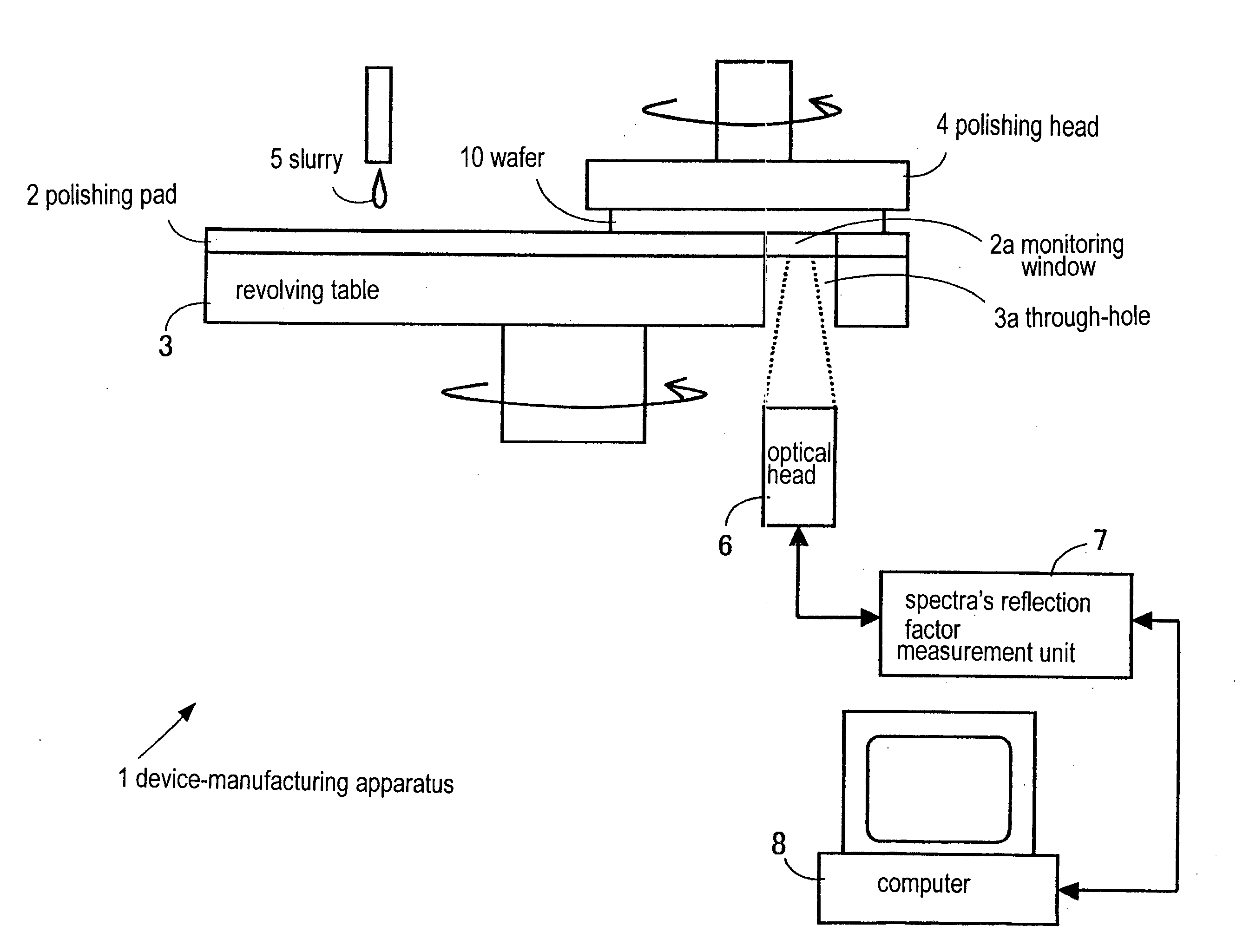
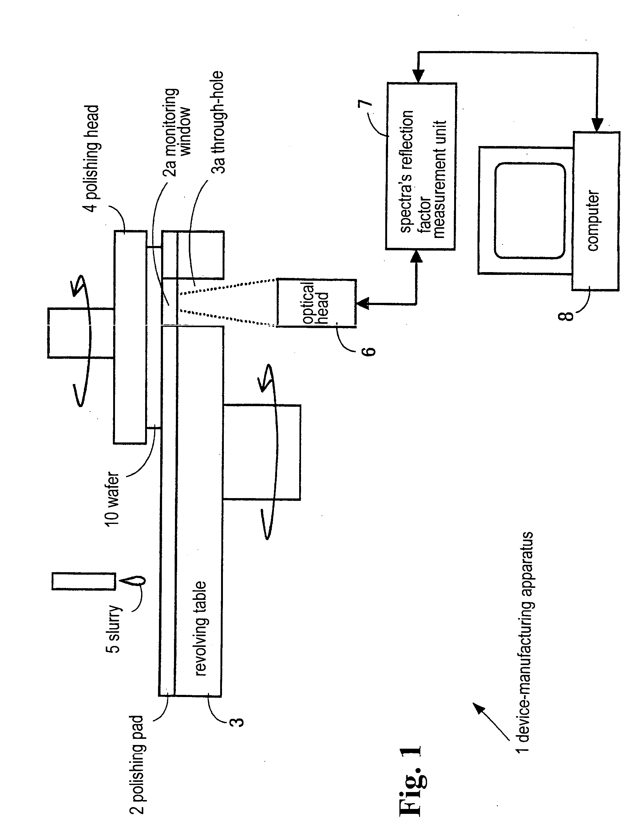
[0026] Hereunder, embodiments of the present invention will be explained with reference to the accompanying drawings. In the embodiments, as an example, an insulating film formed on a wafer is polished during a manufacturing process of a semiconductor device. An optical model for evaluating a film thickness during a polishing process will be explained first.

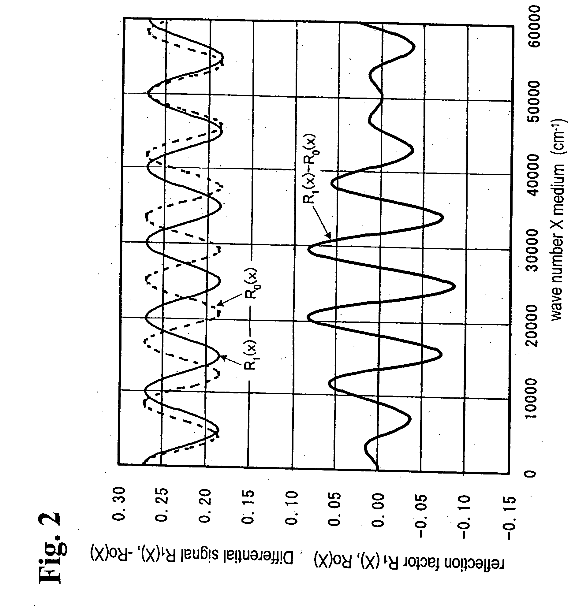
[0027] A thickness of a thin film at a polishing time t is defined as d; a reflection factor of light comprising the wave number x in a medium at the polishing time t is defined as R1(x); a thickness of the thin film at a polishing time t−Δt with a relatively short period of time Δt from the polishing time t is defined as d+Δd; and a reflection factor of light comprising the wave number x in the medium at the polishing time t−Δt is defined as R0(x). The reflection factors R1(x) and R0(x) are individually expressed by optical models (1) and (2) as shown below:

R1(x)=A·cos(4πdx)+B  (1)

R0(x)=A·cos{4π(d+Δd)x}+B  (2)

where A and B ...


PUM


Abstract

A method of evaluating a thickness of a film during a polishing process includes the steps of irradiating light onto a surface of the film during the polishing process; obtaining a differential signal of reflection spectra at a polishing time t and a polishing time t−Δt with a time difference Δt from the polishing time t; and analyzing the differential signal to obtain a thickness d of the film at the polishing time t.

Description

BACKGROUND OF THE INVENTION AND RELATED ART STATEMENT [0001] The present invention relates to a method of evaluating a film thickness, a method of detecting a polishing terminal, and a device-manufacturing apparatus. More particularly, the present invention relates to a method of evaluating a film thickness and a method of detecting a polishing terminal when an insulating film formed on a device is polished with a chemical mechanical polishing method. The present invention also relates to an apparatus for manufacturing a device while evaluating a film thickness. [0002] In a process of manufacturing a semiconductor device, a chemical mechanical polishing (CMP) method has been widely used for polishing an insulating film and a metallic film formed on a wafer. In the CMP method, it is necessary to accurately evaluate an actual thickness of an insulating film or a metallic film during a polishing process and determine a point of terminating the polishing process (polishing terminal). [0...

Claims


Application Information

Patent Timeline
Patent Type & Authority Applications(United States)
IPC IPC(8): B24B49/02B24B37/013B24B49/12H01L21/304H01L21/3105H01L21/4763
CPCB24B37/013H01L21/31053B24B49/12
Inventor FUJIKAKE, SHINJI
Owner FUJI ELECTRIC HLDG CO LTD
Why Eureka
Try Eureka