Stress-induced control of polarization dependent properties in photonic devices

a photonic device and polarization dependent technology, applied in the field of stress-induced control of polarization dependent properties of photonic devices, can solve the problems of stringent requirements, unutilized soi size reduction potential, and high implementation cost, and achieve the effect of enhancing design freedom

Inactive Publication Date: 2005-09-08
NAT RES COUNCIL OF CANADA
View PDF8 Cites 30 Cited by
  • Summary
  • Abstract
  • Description
  • Claims
  • Application Information

AI Technical Summary

Benefits of technology

[0013] The invention makes use of stress fields in the design of waveguides to control polarization dependant loss and polarization dependent refractive index. In accordance with the principles of the invention cladding stress induced birefringence is taken into account in the waveguide design, enabling the birefringence to be decoupled from geometrical constraints. The novel technique achieves the final desired birefringence with a combination of the stress-induced and geometrical birefringence. Waveguide dimensions can thus be optimized to meet other design criteria, giving an enhanced degree of design freedom.

Problems solved by technology

Such devices, however, are of comparable size to those based on glass waveguides, and the size-reduction potential of SOI is unutilized.
This stringent requirement is technologically a challenge and may be very expensive to implement.
It is often impossible to simultaneously meet several design objectives, including zero birefringence, using waveguide dimensions alone.
These are some of the reasons why small-size SOI waveguide devices are not currently available commercially.
The rate of change with dimensions also becomes very large.
Obviously, for waveguides with high geometrical anisotropy (e.g. for W>>H), this particular condition may not be possible to fulfill.
It is often impossible to simultaneously meet several design objectives, including zero birefringence, using waveguide dimensions alone.
Unfortunately, the condition for Δngeo=0 may cease to exist.

Method used


Image

  • Stress-induced control of polarization dependent properties in photonic devices
  • Stress-induced control of polarization dependent properties in photonic devices
  • Stress-induced control of polarization dependent properties in photonic devices

Examples


Embodiment Construction

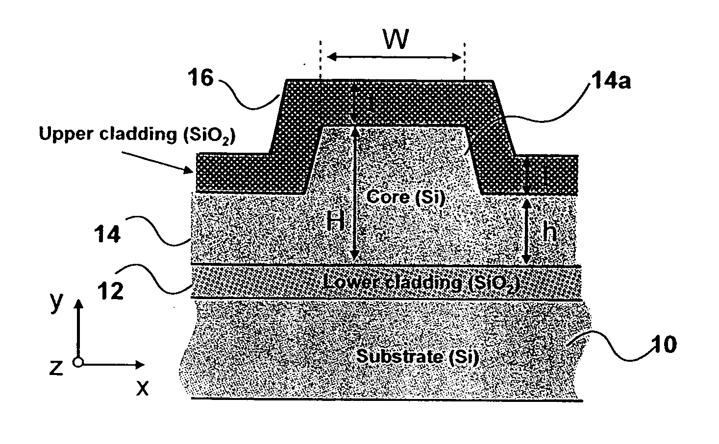
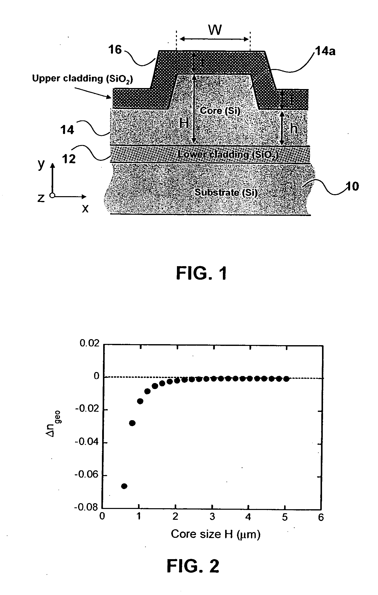
[0030]FIG. 1 shows a typical waveguide structure comprising a silicon substrate 10, a lower SiO2 cladding layer 12, a core layer 14 with ridge 14a, and an upper SiO2 cladding layer 16. The upper cladding 16 has a thickness of t; etch depth is D=H−h.

[0031]FIG. 2 shows the dependence of birefringence on the core thickness H. In this example, the waveguides have the same width as the core thickness H, and are etched to half the thickness. Similar dependence is found in other waveguide cross-sections.

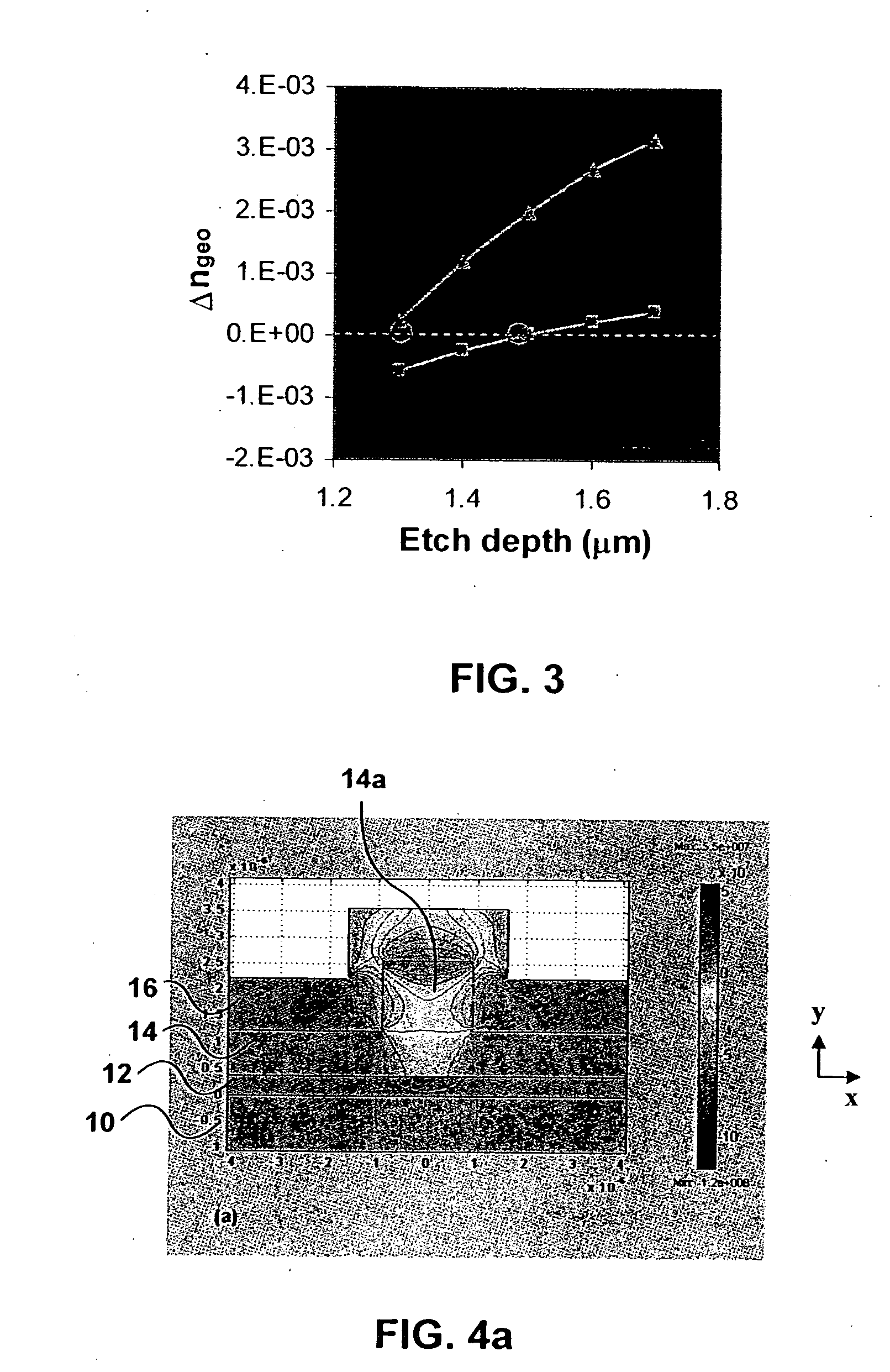
[0032]FIG. 3 shows the variations of Δngeo with the ridge etch depth, for 3 different waveguide widths W. In this example, the core thickness is 2.2 μm. The circles indicate the birefringence-free points.

[0033] In such a waveguide structure stress-induced changes in material refractive indices are given by:

nx−nx0=−C1σx−C2(σy+σz)  (1a)

ny−ny0=−C1σy−C2(σz+σx)  (1b)

[0034] Therefore:

nx−ny=(C1−C2)(σy−σx)  (2)

Here σi is the stress tensor, ni the material refractive index, ni0 the stress-f...


PUM

PropertyMeasurementUnit
sizeaaaaaaaaaa
core sizeaaaaaaaaaa
thickaaaaaaaaaa

Abstract

In order to make a photonic device incorporating a waveguide, a waveguide is formed with a predetermined geometry. Birefringence is then controlled by determining the amount of stress induced within the waveguide.

Description

CROSS REFERENCE TO RELATED APPLICATION [0001] This application claims the benefit under 35 USC 119(e) of U.S. provisional application No. 60 / 547,078 filed on Feb. 25, 2004, the contents of which are incorporated herein by reference.FIELD OF THE INVENTION [0002] This invention relates to photonic devices with controlled polarization dependent properties and methods of making the same. BACKGROUND OF THE INVENTION [0003] In photonic devices incorporating waveguides, mode transmission is affected both by the material anisotropy, and by the cross-sectional geometry of waveguides. An example of the structures under discussion is illustrated schematically in FIG. 1. The waveguides include a core and cladding layers and generally interfaces between the core and cladding layers impose different boundary conditions for modes of propagation with different polarizations. These effects induce a polarization dependent loss (PDL), and a polarization dependent refractive index. [0004] Modes with el...

Claims


Application Information

Patent Timeline
Patent Type & Authority Applications(United States)
IPC IPC(8): B05D5/06C03B37/00G02B6/10
CPCG02B6/105G02B2006/12097G02B6/122
Inventor XU, DAN-XIACHEBEN, PAVELDALACU, DANJANZ, SIEGFRIED
Owner NAT RES COUNCIL OF CANADA
Why Eureka
Try Eureka