Package array and package unit of flip chip LED

Inactive Publication Date: 2005-09-15
OPTO TECH
View PDF6 Cites 148 Cited by
  • Summary
  • Abstract
  • Description
  • Claims
  • Application Information

AI Technical Summary

Benefits of technology

[0007] Another object of the invention is to provide a package array and a package unit of flip chip LED to enhance the packaging integration and effectively solve the heat-radiating problem after packaging.
[0008] Another object of the invention is to provide a flip chip LED package unit, which has a g

Problems solved by technology

However, this kind of LED package array is restricted by the package size of the LED itself so that its volume can't be shrunk.
Moreover, because the heat-radiating path of each LED is only the metal pin, the hea

Method used


Image

  • Package array and package unit of flip chip LED
  • Package array and package unit of flip chip LED
  • Package array and package unit of flip chip LED

Examples


Embodiment Construction

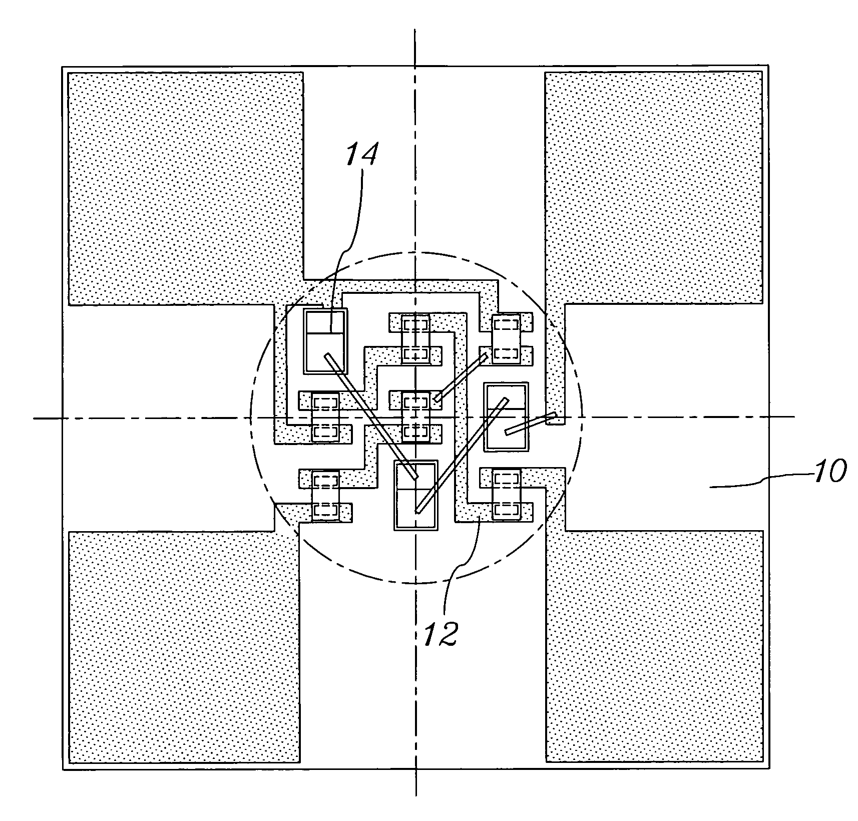
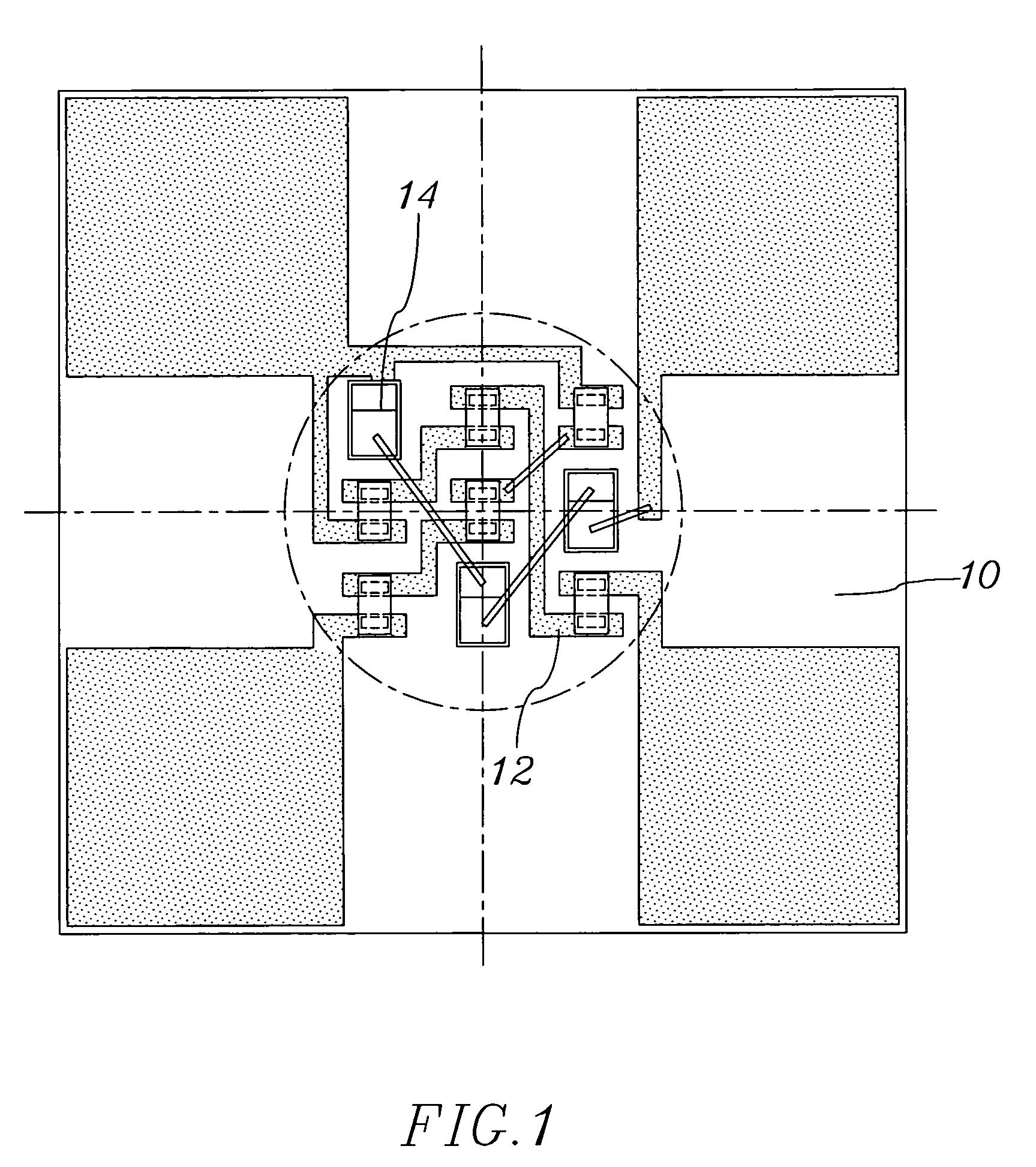
[0018] In an LED chip, an LED epitaxy layer having a PN junction is formed on a GaN, sapphire, GaP or GaAs substrate, and two electrodes are electroplated at appropriate positions to provide an enough voltage difference between two ends of the epitaxy layer of the LED so that light can be generated in the PN junction on the epitaxy layer and then emitted out. In the invention, the LED chip is mounted on a ceramic material capable of enduring the eutectic temperature of the fabrication process for packaging. Metal wires are then directly distributed on the ceramic material to finish an LED package unit. Or a plurality of LEDs are serial / parallel connected together to finish a high density package array.

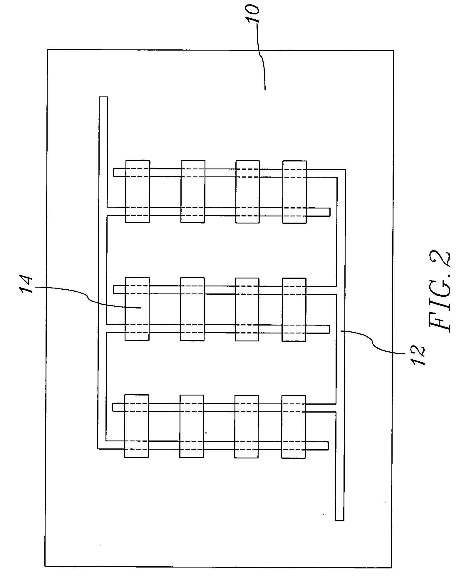
[0019]FIG. 1 shows a flip chip LED package array of the invention, wherein a metal wire layer 12 is distributed on the surface of a ceramic substrate 10. The ceramic substrate 10 is made of a material capable of enduring the eutectic temperature of the fabrication process and matching...


PUM


Abstract

A package array and its package unit of flip chip LED are proposed, wherein an LED chip is mounted on a ceramic material capable of enduing the eutectic temperature of the fabrication process for packaging. Next, metal wires are directly distributed on the ceramic material to finish an LED package unit, or a plurality of LEDs are serial/parallel connected with metal wires on the ceramic material to finish a high density package array. Because the ceramic material has a good thermal expansion match and a good thermal conductivity and the LED chip itself has a high reflective index match, the light emission characteristic and heat-radiating effect of the packaged LED can be effectively improved.

Description

FIELD OF THE INVENTION [0001] The present invention relates to a package technique of flip chip LED and, more particularly, to a high density package array and its package unit of flip chip LED making use of a ceramic material having a good thermal expansion match. BACKGROUND OF THE INVENTION [0002] The light emission principle of LED bases on inherent characteristics of semiconductor. Different from incandescence lamps, in an LED, light will be emitted when a current flows forwards into the PN junction of semiconductor. Therefore, LEDs are called cold lights. Because LEDs have the advantages of high durability, long lifetime, light weight, low power consumption and no noxious materials like mercury, they have been widely used in the illumination industry. Usually, LEDs are packaged in array to be used in electronic billboards and traffic signs. [0003] A conventional LED package array comprises a plurality of LEDs, each LED having a chip mounted on a leadframe. A molding compound co...

Claims


Application Information

Patent Timeline
IPC IPC(8): H01L29/22
CPCH01L24/13H01L2924/01322H01L24/45H01L24/48H01L24/81H01L25/0753H01L33/641H01L2224/13144H01L2224/16245H01L2224/451H01L2224/48091H01L2224/73265H01L2224/81805H01L2924/09701H01L2924/15787H01L2924/19107H01L2924/12032H01L2924/1815H01L2924/01014H01L2924/01013H01L2924/12041H01L24/16H01L2924/00014H01L2924/0105H01L2924/00H01L2924/12036
Inventor LIN, MING-DERLIN, SAN-BAO
Owner OPTO TECH
Why Eureka
Try Eureka