Semiconductor package having heat spreader and package stack using the same

Active Publication Date: 2005-09-15
SAMSUNG ELECTRONICS CO LTD
View PDF7 Cites 28 Cited by
  • Summary
  • Abstract
  • Description
  • Claims
  • Application Information

AI Technical Summary

Benefits of technology

[0015] Yet another embodiment provides a chip mounted on an upper surface of a board with a heat spreader mounted on a lower surface of the board. External contact terminals protrude a height greater than the combined height of the chip and heat spreader from the lower surface of the board. A predetermined number of external contact terminals protrude through and connect with ground holes in the heat spreader. The remaining external contact terminals are vertically exposed by the heat spreader. A top heat spreader can be attached to the rear side of the chip and ground bumps can connect contac

Problems solved by technology

A semiconductor package suitable for high speed and performance generates a large quantity of heat during the operation, which results in degeneration of performance.
However, since the heat spreaders in the prior art have a structure where a thermal conductive pad is simply attached on the rear side of a molding body or a semiconductor chip, the prior art merely improved heat dissipation while not improving electrical performance.
This kind of structure in the prior a

Method used


Image

  • Semiconductor package having heat spreader and package stack using the same
  • Semiconductor package having heat spreader and package stack using the same
  • Semiconductor package having heat spreader and package stack using the same

Examples


Example

First Exemplary Embodiment

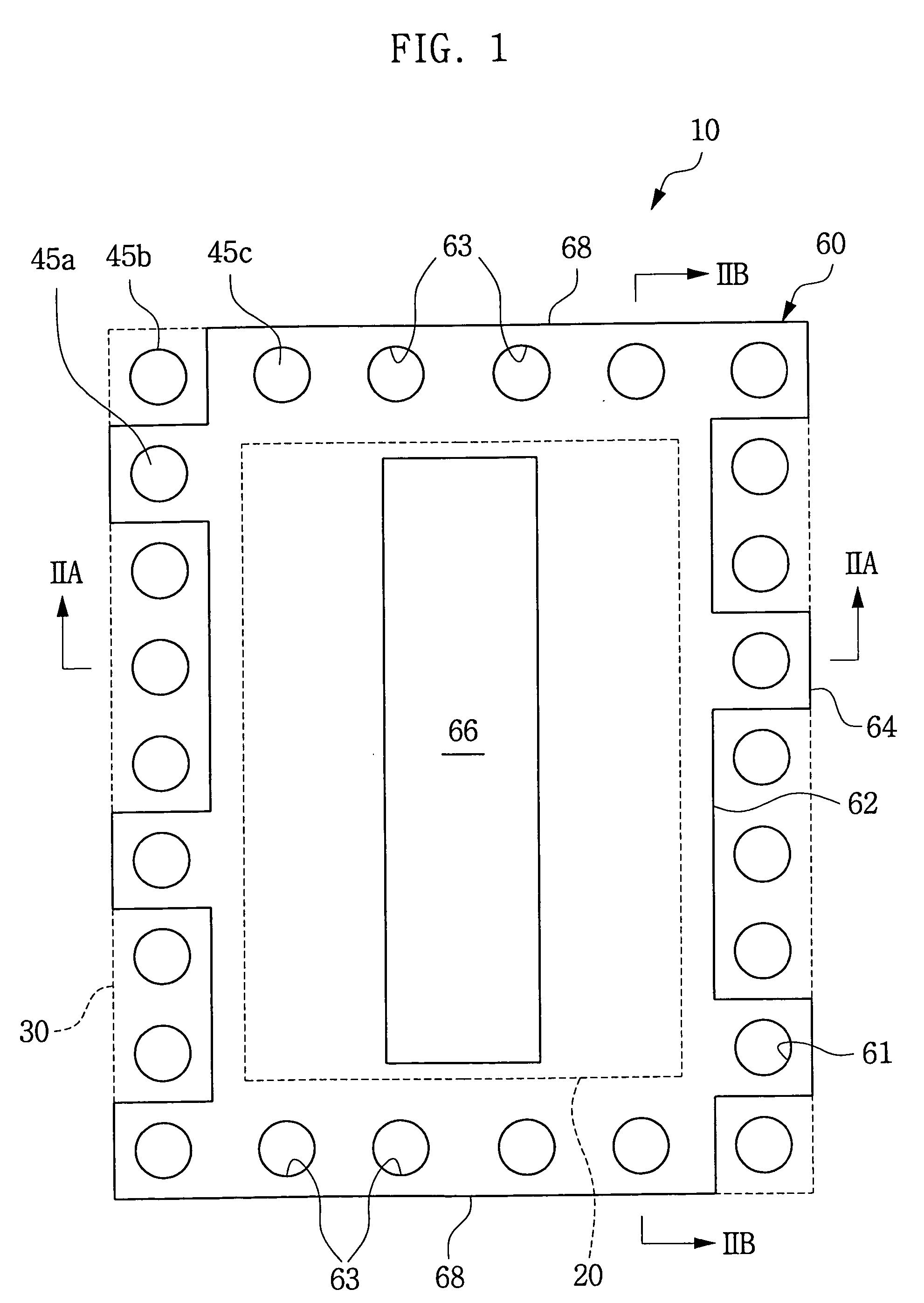
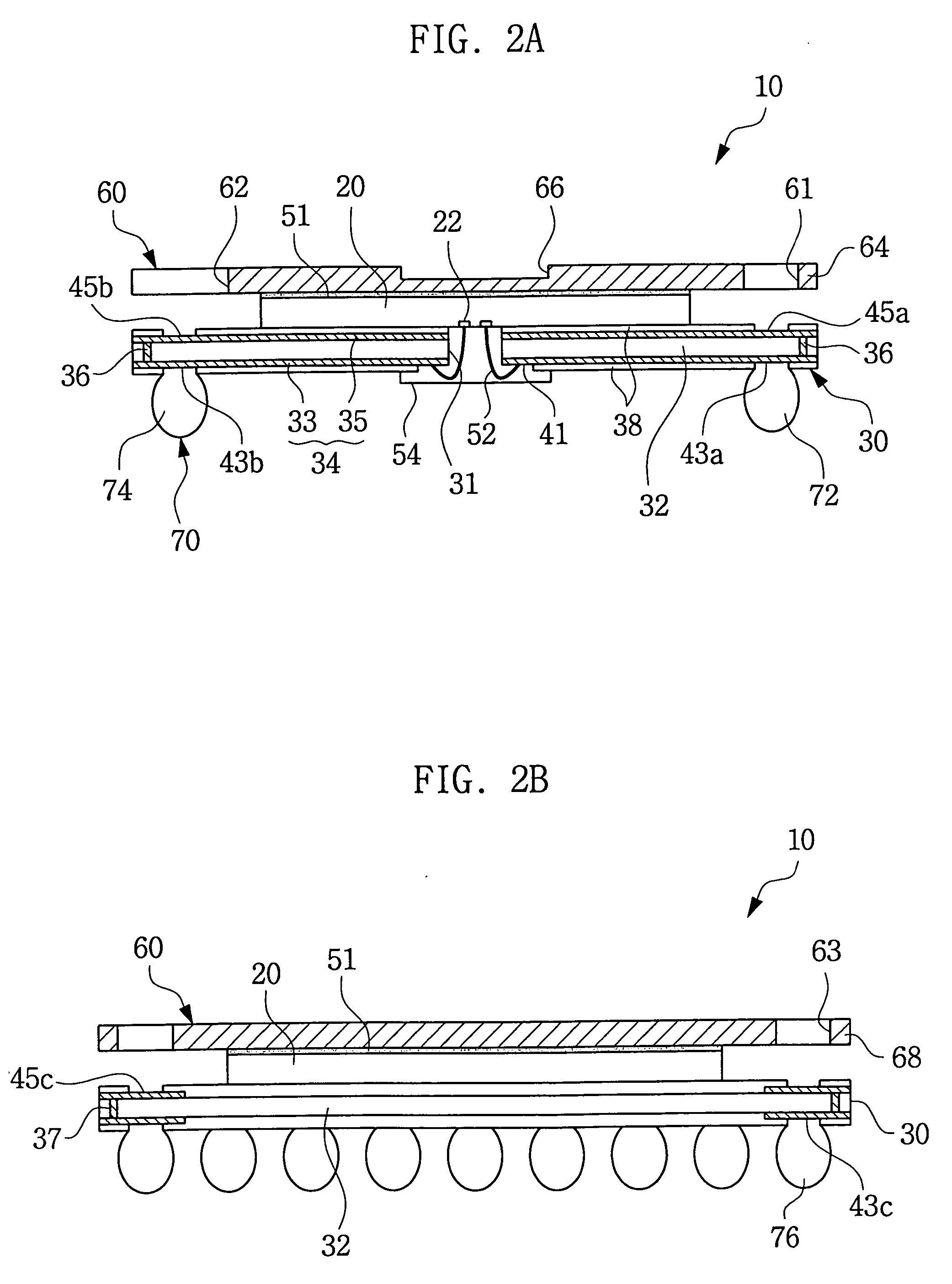
[0039]FIG. 1 is a plan view of a semiconductor package having heat spreader according to a first exemplary embodiment of the present invention. FIG. 2A is a cross-sectional view taken along the line IIA-IIA in FIG. 1. FIG. 2B is a cross-sectional view taken along the line IIB-IIB in FIG. 1.

[0040] Referring to FIGS. 1 through 2B, in the semiconductor package 10, according to the first exemplary embodiment of the present invention, the semiconductor chip 20 is mounted on and connected with the board 30 with its active surface facing the upper surface of the board 30. The heat spreader 60 is attached to the rear side of the semiconductor chip 20. And the external terminals 70 are formed on the peripheral part of the lower surface of the board 30.

[0041] More specifically, the semiconductor chip 20 is a center pad type, of which bonding pads 22 are formed on the center region of the active surface. Generally, a center pad type semiconductor chip is more favor...

Example

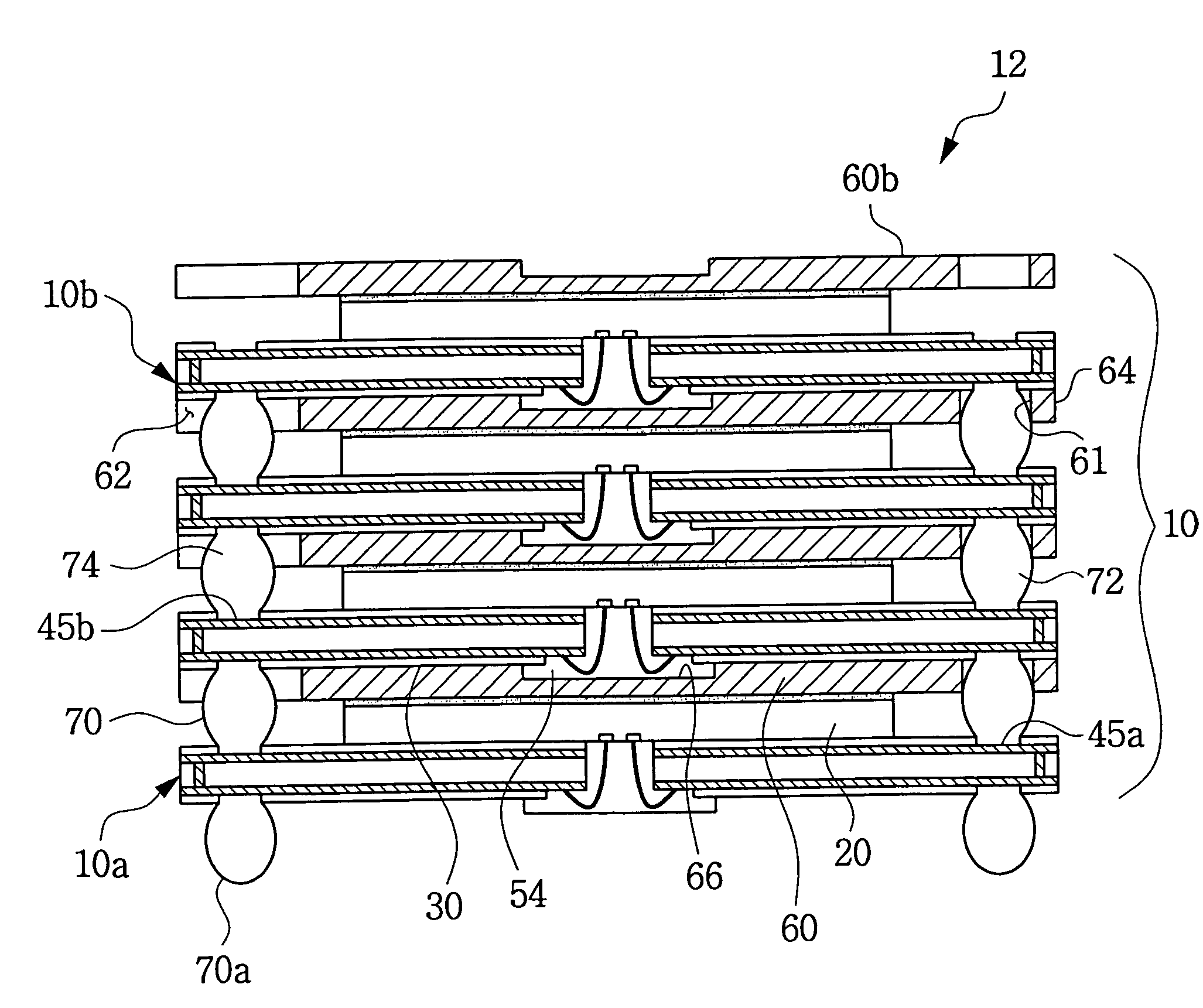
[0055]FIG. 5 shows a package stack 16 of the second embodiment formed by using the semiconductor packages 10 and 14 according to the first and second embodiments. Referring to FIG. 5, the package stack 16 according to the second embodiment stacks three semiconductor packages 10 according to the first embodiment. Further, the package stack 16 stacks the semiconductor package 14 on top thereof. The package stack which stacks at least one semiconductor package according to the first embodiment and the semiconductor package according to the second embodiment on the top thereof is only a variant of the package stack according to the second embodiment.

[0056] The heat spreader 60 of the semiconductor package 14 shown in FIG. 5 on top of the package stack 16 according to the second embodiment is grounded, whereas the heat spreader 60b of the uppermost semiconductor package 10b on top of the package stack 12 shown in FIG. 3 according to the first embodiment is not grounded. Therefore, the h...

Example

[0058] According to the third exemplary embodiment, referring to FIG. 6, a semiconductor chip 120 is flip chip bonded on the upper surface of a board 130, a heat spreader 160 is attached on the rear side of the semiconductor chip 120, and external contact terminals 170 are formed on the lower surface of the board 130. The flip chip bonded part is covered with epoxy resin 129 provided by the under-fill method.

[0059] More specifically, electrode bumps 128 are each attached to a bonding pad 122 for flip chip bonding in the semiconductor chip 120.

[0060] The board 130 may be a circuit board having metal wiring layer 134 on a substrate body 132. The board 130 may include a tape wiring board, a printed circuit board (PCB) or a ceramic board. Although there is an example of the metal wiring layer 134 being formed on both sides of the board 130 according to the third exemplary embodiment, it is also possible to form at least one or more metal wiring layers within the board 130. The substra...


PUM


Abstract

A semiconductor package which can be stacked to form a package stack that includes a semiconductor chip with bonding pads, a board having contact pads on its upper surface and bump pads on its lower surface, a heat spreader attached to the rear side of the semiconductor chip and covering the upper surface of the board, and external contact terminals including ground terminals and signal terminals formed on the bump pads. The contact pads of the board include ground contact pads connected with the ground terminals and signal contact pads connected with the signal terminals. The heat spreader includes indented parts to expose the signal contact pads and protruded parts to cover the ground contact pads which are exposed through holes formed on the protruded parts on the peripheral part of the heat spreader. The semiconductor package can alternatively have the heat spreader attached to the lower surface of the board.

Description

CROSS REFERENCE TO RELATED APPLICATIONS [0001] This U.S. non-provisional application claims priority under 35 U.S.C. §119 to Korean Patent Application No. 2004-16179 filed Mar. 10, 2004, the contents of which are incorporated herein in its entirety by reference. BACKGROUND OF THE INVENTION [0002] 1. Field of the Invention [0003] The present invention relates generally to a semiconductor package and a package stack using the same and, more particularly, to a semiconductor package having a heat spreader and a package stack using the same. [0004] 2. Description of the Related Art [0005] The electronics industry continues to seek products that are lighter, faster, smaller, multi-functional, more reliable and more cost-effective. One of the important technologies making these objectives possible is semiconductor packaging technology by which a chip scale package (CSP) was recently realized. CSP technology provides a small sized package having the size level of a semiconductor chip. [0006...

Claims


Application Information

Patent Timeline
IPC IPC(8): H01L23/36H01L23/02
CPCH01L23/13H01L23/3157H01L2924/07802H01L2924/15151H01L2225/1088H01L2224/73253H01L2224/73215H01L2224/32225H01L2924/3025H01L2924/15331H01L2924/01079H01L2225/1094H01L2225/1058H01L23/552H01L24/16H01L24/29H01L24/32H01L24/48H01L24/73H01L25/105H01L2224/16225H01L2224/291H01L2224/2919H01L2224/32245H01L2224/48091H01L2224/4824H01L2224/73204H01L2224/73265H01L2225/1023H01L2924/00014H01L2924/00H01L2224/05026H01L2224/05573H01L2224/05599H01L2224/45099H01L2924/00012H01L2224/45015H01L2924/207E01H1/005
Inventor LEE, JONG-JOOSONG, YOUNG-HEE
Owner SAMSUNG ELECTRONICS CO LTD
Why Eureka
Try Eureka