In-plane switching mode liquid crystal display device and fabrication method thereof

a liquid crystal display and switching mode technology, applied in the direction of propelling pencils, instruments, printing, etc., can solve the problems of poor contrast ratio of screen, disadvantage of tn mode lcd, and some 90° viewing angle, so as to reduce resistance and enhance the effect of screen contrast ratio

Active Publication Date: 2005-09-15
LG DISPLAY CO LTD
View PDF11 Cites 43 Cited by
  • Summary
  • Abstract
  • Description
  • Claims
  • Application Information

AI Technical Summary

Benefits of technology

[0018] Therefore, an object of the present invention is to provide an in-plane switching (IPS) mode liquid crystal display (LCD) capable of reducing resistance and enhancing a contrast ratio of a screen by forming a common electrode and a pixel electrode as a dual layer of transparent electrode and to provide opaque electrode, and a fabrication method of such LCD.

Problems solved by technology

The TN mode LCD is, however, disadvantageous in that its viewing angle is some 90°, which is quite narrow.
However, the in-plane mode LCD with the 2ITO structure has a problem in that since the electrodes are made of the transparent material, they do not exhibit complete black luminance in a normally black mode and thus a contrast ratio of a screen is not good.
In fabricating a liquid crystal display panel, the larger the panel becomes, the resistance of the electrodes increases which in turn affects the picture quality.
In this respect, changing the structure of the existing design of the LCD cannot solve the resistance problem.
In particular, the resistance of the transparent electrodes creates a big problem.
If the electrodes are made thick in order to lower the resistance of the electrodes, the liquid crystal molecules manifest abnormal behavior due to a step according to the thickness of the electrodes, thereby degrading the picture quality, e.g., due to light leakage.

Method used


Image

  • In-plane switching mode liquid crystal display device and fabrication method thereof
  • In-plane switching mode liquid crystal display device and fabrication method thereof
  • In-plane switching mode liquid crystal display device and fabrication method thereof

Examples


first embodiment

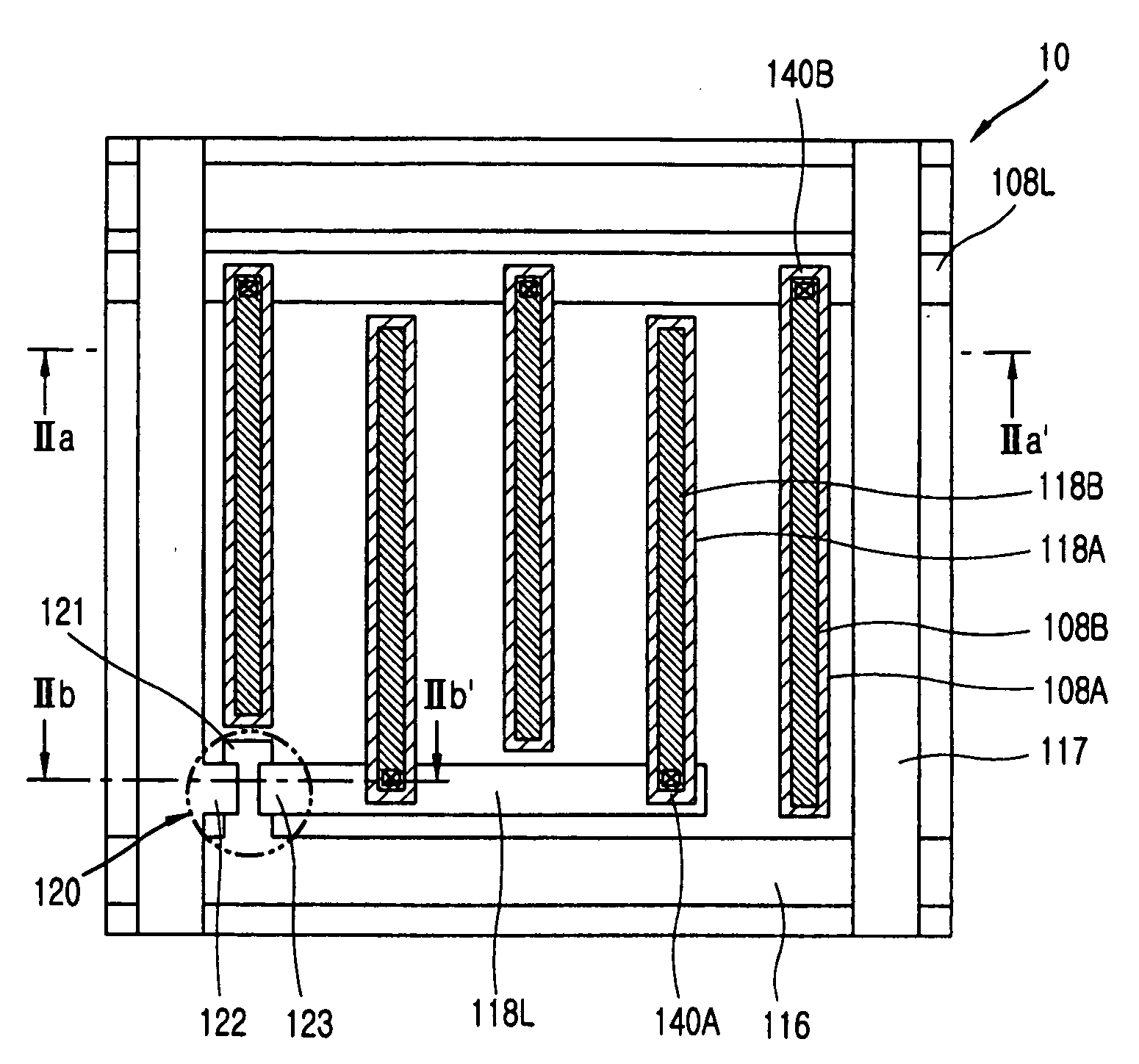
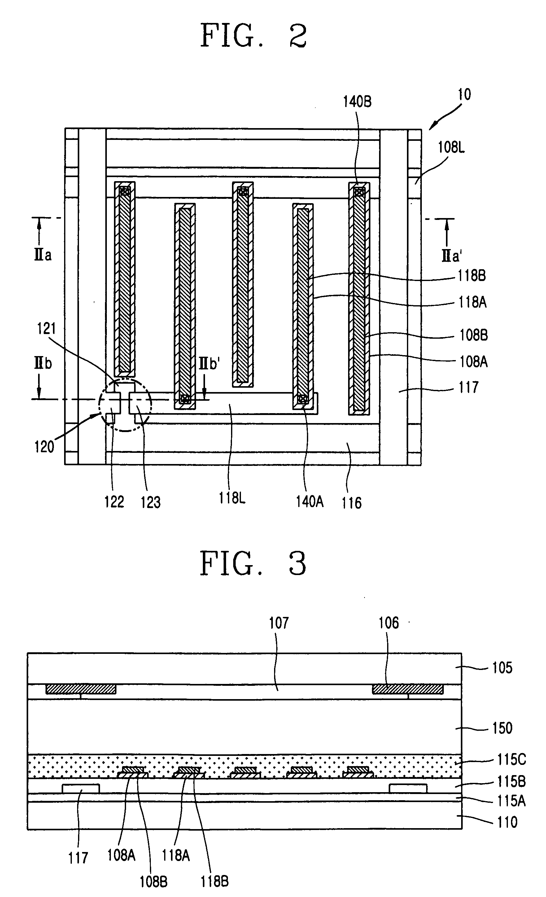
[0034]FIG. 2 is a plan view showing a portion of an array substrate of an IPS mode LCD in accordance with the present invention. In the LCD, a N-number of gate lines and a M-number of data lines cross to form a N×M number of pixels, but for the sake of explanation and clarity, only one pixel is shown in FIG. 2.

[0035] As shown in FIG. 2, a gate line 116 and a data line 117 are arranged vertically and horizontally to form a pixel region on a transparent glass substrate 110. A thin film transistor (TFT) 120 (a switching device) is formed at the crossing of the gate line 116 and the data line 117.

[0036] The TFT 120 includes a gate electrode 121 connected to the gate line 116, a source electrode 122 connected to the data line 117, and a drain electrode 123 connected to a pixel electrode line 118L. The TFT 120 also includes an insulation film for insulating the gate electrode 121 and the source / drain electrodes 122 and 123, and an active layer (a channel layer) for forming a conductive c...

second embodiment

[0081]FIG. 7A is a plan view showing a portion of an array substrate of an IPC mode LCD in accordance with the present invention, and FIG. 7B is a sectional view taken along line VII-VII′ of the array substrate of FIG. 7A.

[0082] An array substrate of the second embodiment of the present invention has the same construction as that of the first embodiment except for the structure of the common electrode and the pixel electrode. Thus, the description on the same construction is omitted or brief and only the common electrode and pixel electrode will be described.

[0083] As shown in FIG. 7A, a gate line 216 and a data line 217 defining a pixel region are formed vertically and horizontally on a transparent glass substrate 210, and a TFT 220 is formed at the crossing of the gate line 216 and the data line 217.

[0084] A common electrode 208A and 208B and a pixel electrode 218A and 218B each formed as a dual layer are alternatingly disposed to generate a horizontal electric field in the pixe...

third embodiment

[0092]FIG. 8 is a plan view showing a portion of an array substrate of an IPC mode LCD in accordance with the present invention.

[0093] As shown, a common electrode 308A and 308B and a pixel electrode 318A and 318B each formed as a dual layer are alternatingly disposed in order to generate a horizontal electric field in a pixel region.

[0094] A transparent electrode is used as a first common electrode 308A and a first pixel electrode 318A positioned at a lower side of the dual layer, and an opaque electrode is used as a second common electrode 308B and a second pixel electrode 318B positioned at an upper side of the dual layer. The opaque electrodes 308B and 318B are formed narrower in width than the transparent electrodes 308A and 318A, thereby forming the dual layer structure.

[0095] The common electrodes 308A and 308B and the pixel electrodes 318A and 318B each have a zigzag form (or herringbone structure). With this zigzag form of the common electrodes 308A and 308B and the pixel...


PUM

PropertyMeasurementUnit
viewing angleaaaaaaaaaa
angleaaaaaaaaaa
electric fieldaaaaaaaaaa

Abstract

An IPS (In-Plane Switching) mode LCD (Liquid Crystal Display) includes first and second substrates facing each other; a plurality of gate lines and data lines arranged in a matrix configuration on the first substrate and defining a plurality of pixel regions; at least one common electrode and one pixel electrode alternatingly disposed at the pixel region to generate a horizontal electric field, at least one of them having a structure of a dual layer; and a liquid crystal layer formed between the first and second substrates.

Description

[0001] This application claims the priority benefit of the Korean Patent Application No. 10-2004-0016641 filed on Mar. 11, 2004, which is hereby incorporated by reference. BACKGROUND OF THE INVENTION [0002] 1. Field of the Invention [0003] The present invention relates to an in-plane switching (IPS) mode LCD (Liquid Crystal Display) device and, more particularly, to an IPS mode LCD device in which a common electrode and a pixel electrode are formed as a dual layer of a transparent electrode and an opaque electrode, and to the fabrication method of the IPS mode LCD device. [0004] 2. Description of the Related Art [0005] Recently, as interests on information displays and demands for using a portable (mobile) information medium are increasing, research on and commercialization of a light thin film type flat panel display (FPD), which can substitute the existing display device CRT, are actively ongoing. [0006] Among the FPDs, in particular, an LCD, a device for expressing an image by us...

Claims


Application Information

Patent Timeline
Patent Type & Authority Applications(United States)
IPC IPC(8): G02F1/1343G02F1/133G02F1/136
CPCG02F1/13439G02F1/134363B43K21/02B43K24/08
Inventor AHN, JI YOUNG
Owner LG DISPLAY CO LTD
Why Eureka
Try Eureka