Cross-bar matrix with LCD functionality

a cross-bar matrix and functionality technology, applied in the field of integrated circuit input/output circuits, can solve problems such as difficult to overcome dilemmas and inacceptable solutions

Inactive Publication Date: 2005-09-22
SILICON LAB INC
View PDF3 Cites 3 Cited by
  • Summary
  • Abstract
  • Description
  • Claims
  • Application Information

AI Technical Summary

Problems solved by technology

A problem exists when there are more signals or functions than corresponding pins available to the integrated circuit.
Although this limited I / O pin sharing feature provides a certain degree of flexibility, there exists other situations in which this solution is not acceptable.
In both applications, the dilemma is not easily overcome.

Method used


Image

  • Cross-bar matrix with LCD functionality
  • Cross-bar matrix with LCD functionality
  • Cross-bar matrix with LCD functionality

Examples


Embodiment Construction

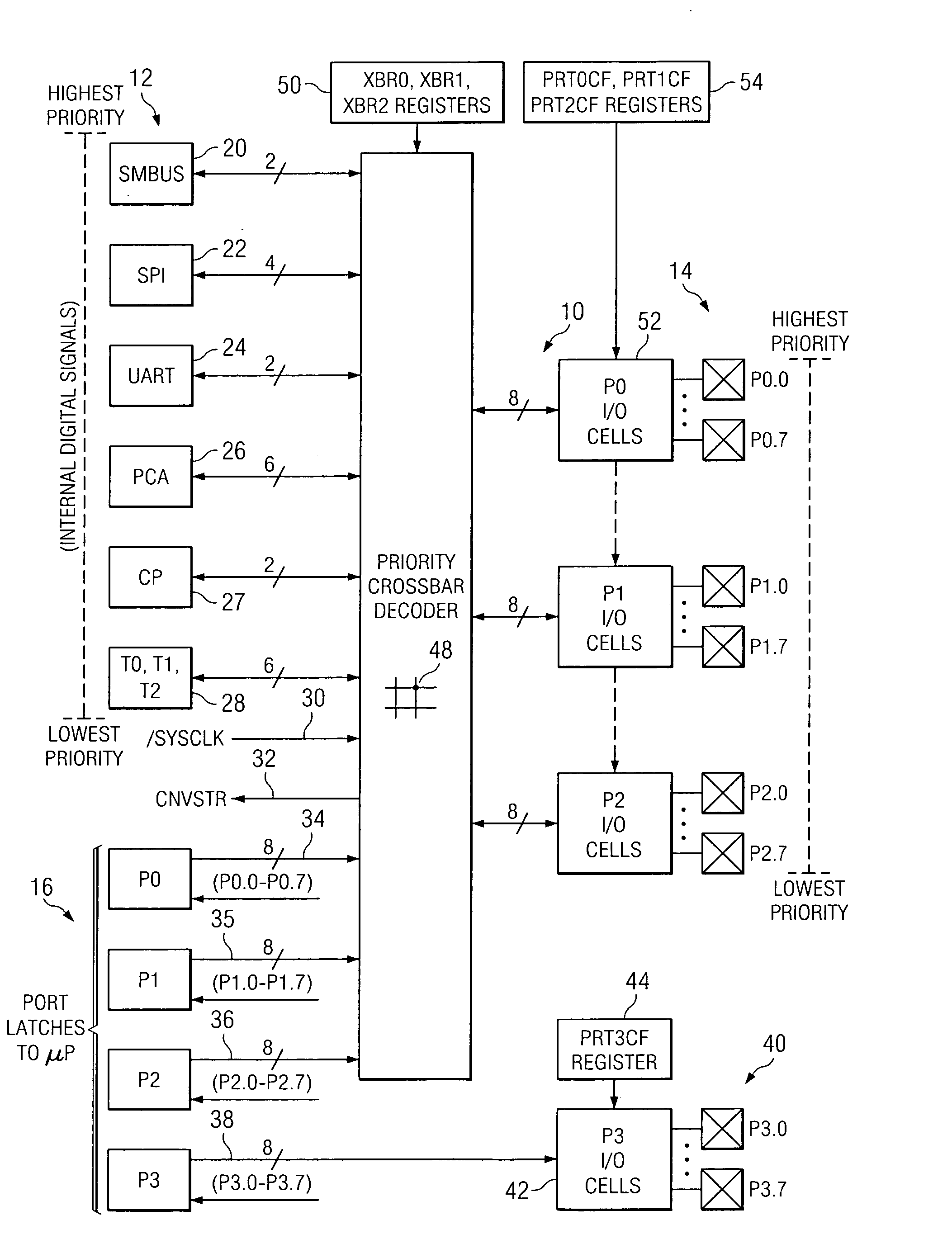
[0024]FIG. 1 illustrates the various digital resources and other support circuits of a semiconductor chip that can be employed and otherwise controlled by a microprocessor (not shown) on the same chip. The aim of any processor system is to couple the digital resources, as well as the I / O ports of the processor itself, to the terminal pins associated with the semiconductor chip. As noted above, most pins of microprocessor chips are assigned one or two functions, but are limited to such functions. This represents a major shortcoming, especially if the semiconductor chip is small in area, thereby leaving very little room for I / O pins.

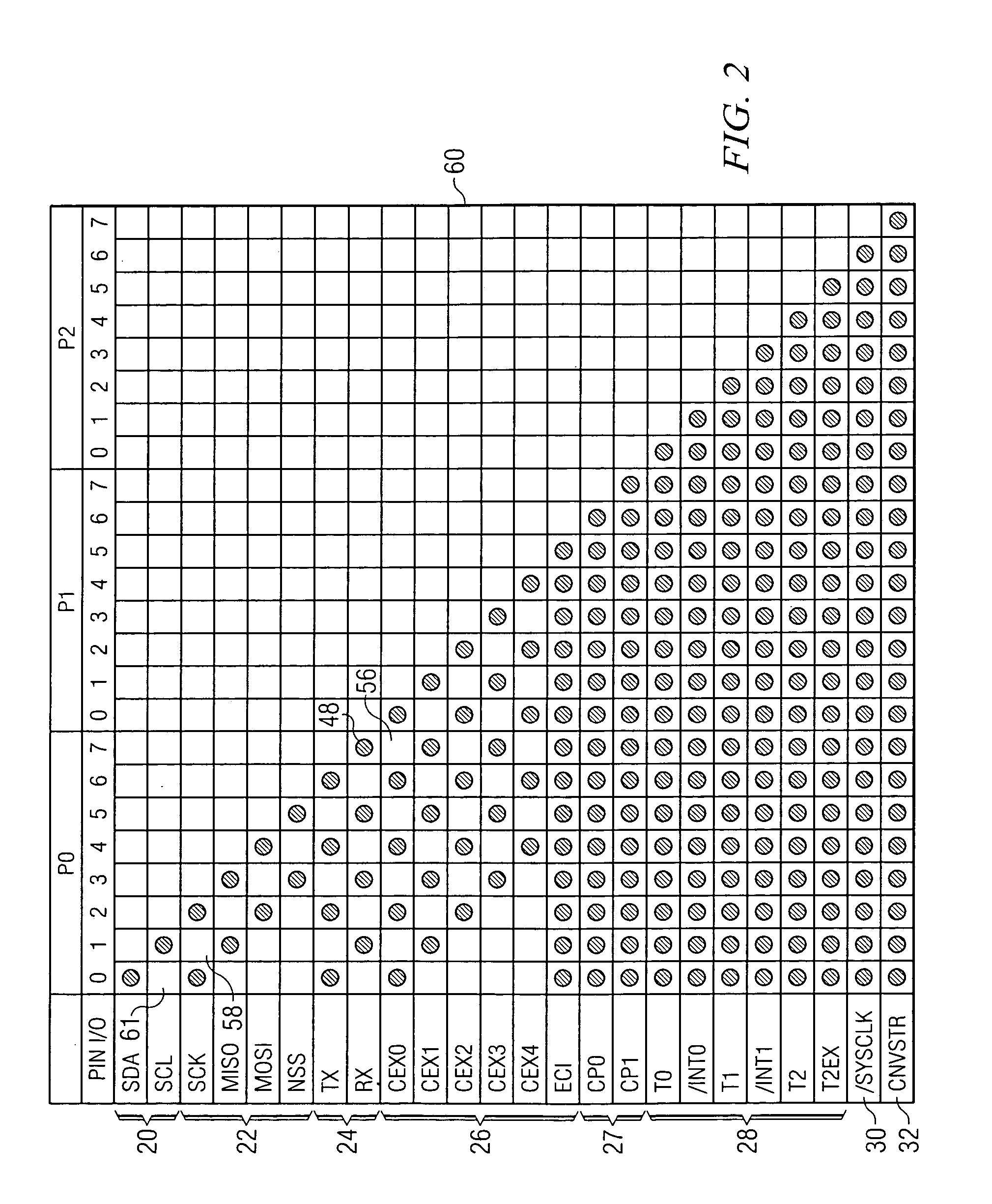
[0025] In FIG. 1, there is shown a priority cross-bar decoder 10 for coupling the digital resources 12 to the various I / O pins 14 of the chip. The priority of each I / O pin is shown. The various digital resources 12, from the highest to lowest priority, include two bits of a system management bus 20, four bits of a serial peripheral interface 22, two bits ...


PUM


Abstract

A cross-bar matrix includes a plurality of matrix cells arranged in rows and columns wherein each row of cells is associated with a signal input and each column of cells is associated with a common signal output. An enable input controls whether at least a portion of the cells couple a signal on the associated common signal input to a signal output associated with a cell or couple an LCD signal to a signal output and exclude control of the at least portion of said plurality of cells by the control input.

Description

RELATED APPLICATION [0001] This application is a Continuation in Part of U.S. application Ser. No. 10 / 847,632 filed on May 17, 2004 titled CROSS-BAR MATRIX FOR CONNECTING DIGITAL RESOURCES TO I / O PINS OF AN INTEGRATED CIRCUIT, which is a Continuation of U.S. Pat. No. 6,738,858 issued on May 18, 2004 entitled CROSS-BAR MATRIX FOR CONNECTING DIGITAL RESOURCES TO I / O PINS OF AN INTEGRATED CIRCUIT, and is related to U.S. application Ser. No. 09 / 584,308 entitled PRIORITY CROSS-BAR DECODER.TECHNICAL FIELD OF THE INVENTION [0002] The present invention relates in general to integrated circuit input / output circuits, and more particularly to a matrix arrangement for providing switched access of a plurality of signals and an LCD driver to I / O ports. BACKGROUND OF THE INVENTION [0003] The large scale integration of a number of devices or circuits allows numerous functions to be carried out within a single integrated circuit. On the one hand, semiconductor dies or chips can be made larger to acc...

Claims


Application Information

Patent Timeline
Patent Type & Authority Applications(United States)
IPC IPC(8): H03K19/173H03M7/00
CPCH03K19/1731
Inventor HOLBERG, DOUGLAS R.FERNALD, KENNETH W.
Owner SILICON LAB INC
Why Eureka
Try Eureka