Semiconductor device and manufacturing method of the same

a semiconductor and semiconductor technology, applied in the field of semiconductor devices, can solve problems such as lowering the cutting accuracy of dicing

Active Publication Date: 2005-09-22
SEMICON COMPONENTS IND LLC
View PDF10 Cites 48 Cited by
  • Summary
  • Abstract
  • Description
  • Claims
  • Application Information

AI Technical Summary

Problems solved by technology

However, conventionally, it has been difficult to align the dicing blade on...

Method used


Image

  • Semiconductor device and manufacturing method of the same
  • Semiconductor device and manufacturing method of the same
  • Semiconductor device and manufacturing method of the same

Examples


Embodiment Construction

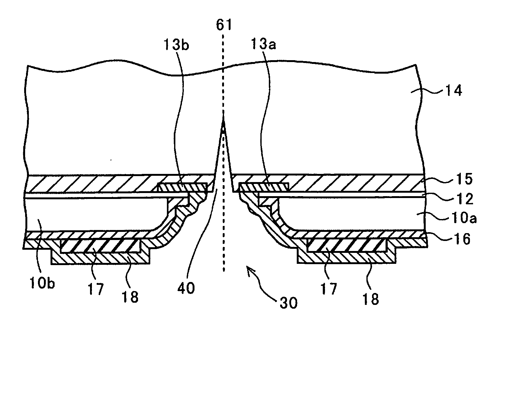
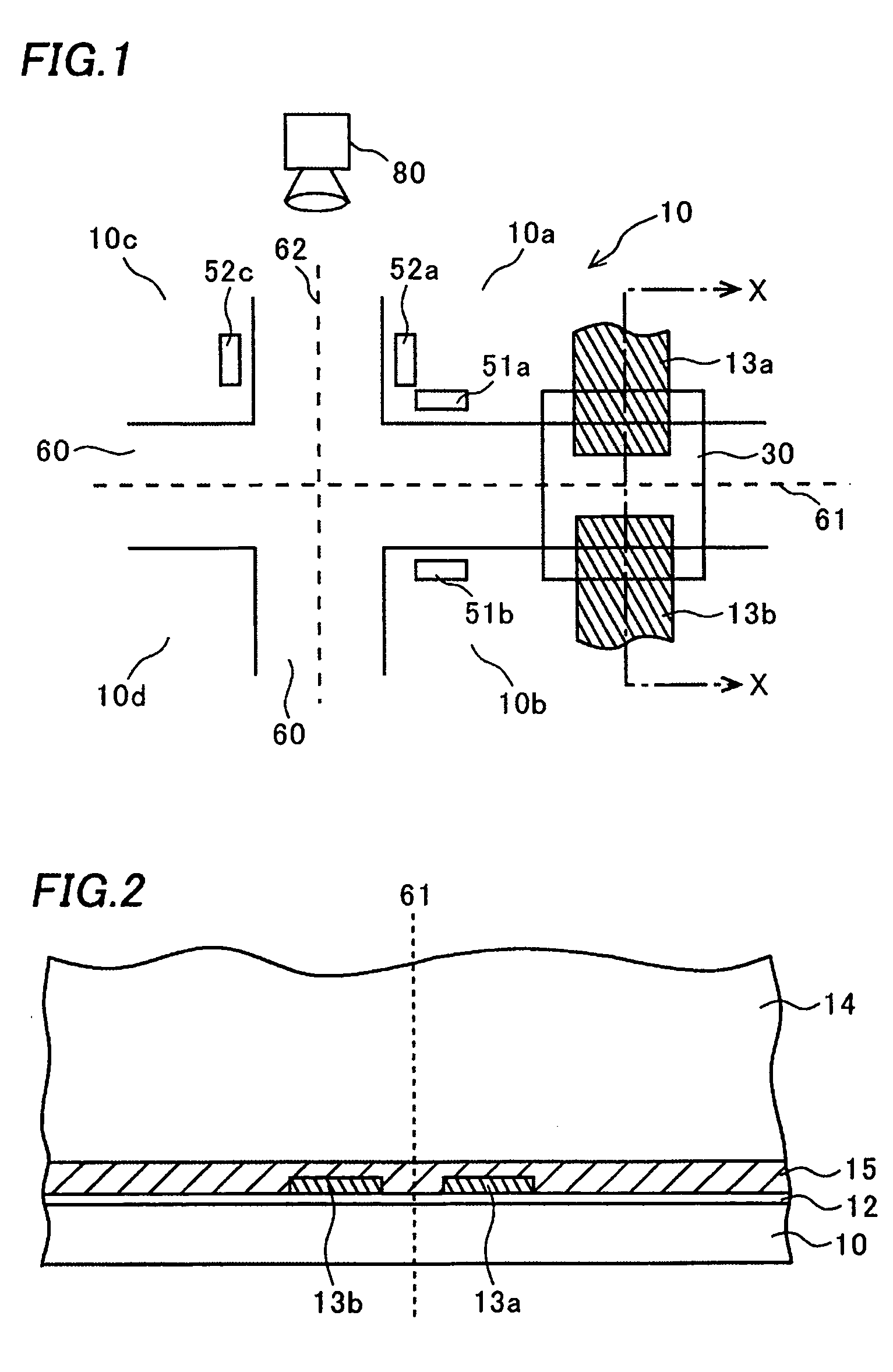
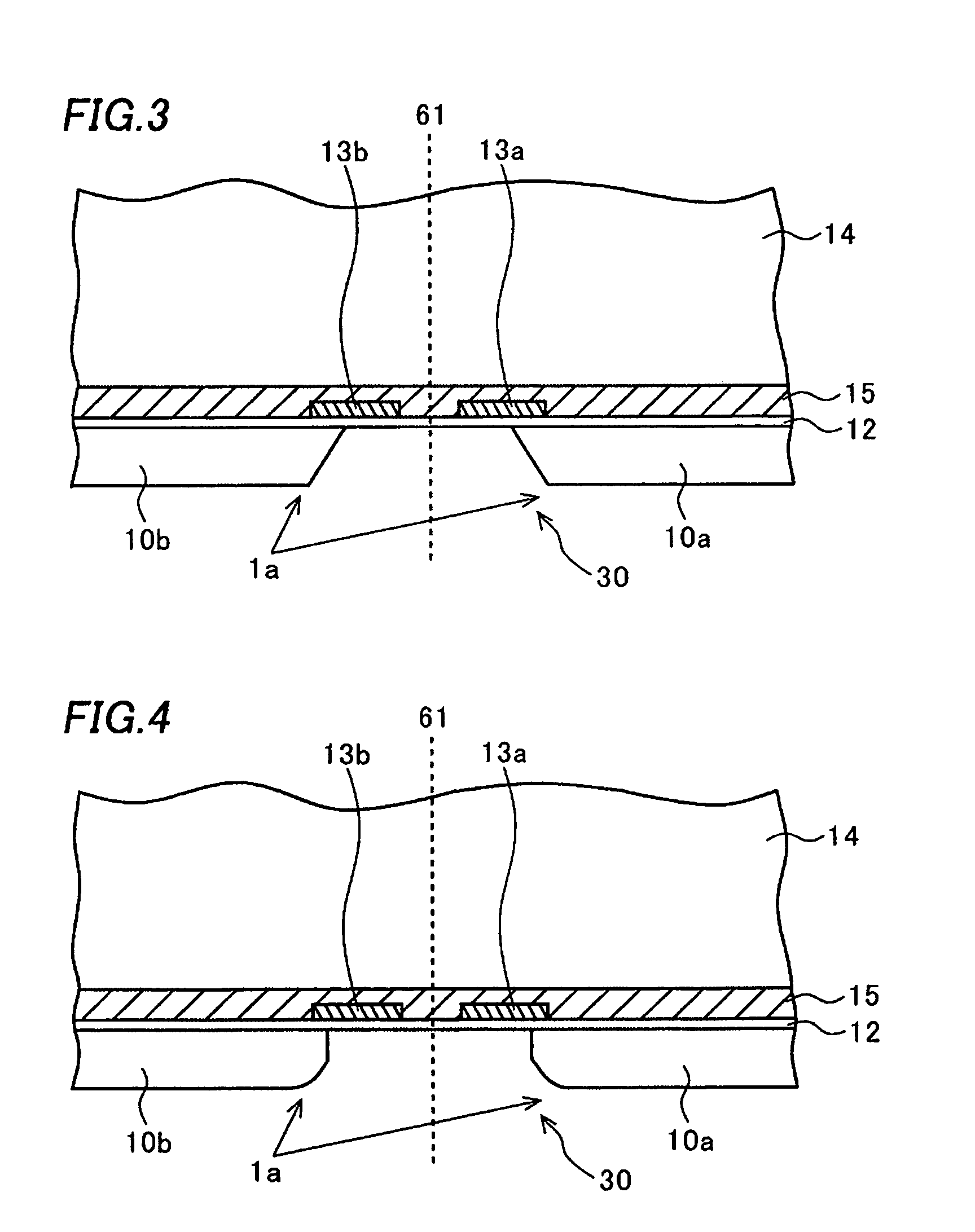
[0021] A manufacturing method of a semiconductor device of an embodiment of the invention will be described with reference to a plan view of FIG. 1. FIG. 1 is a top view of a semiconductor wafer 10 during processing to manufacture the semiconductor device of the embodiment. Note that the front surface of the wafer 10 is shown in FIG. 1 with dice regions, and the back surface of the wafer 10 is attached to a supporting member (not shown in FIG. 1).

[0022] As shown in FIG. 1, semiconductor die regions 10a, 10b, 10c, and 10d and other semiconductor die regions (not shown), which will be individual semiconductor dies by separating the semiconductor wafer 10, are disposed along dicing regions 60 perpendicularly crossing each other. First wirings 13a and 13b which are pads extending from circuits (not shown) formed on the semiconductor die regions are formed in the adjacent semiconductor die regions 10a and 10b, respectively, along the dicing region of the semiconductor wafer. In a positi...


PUM


Abstract

The invention is directed to an improvement of cutting accuracy in a cutting process when a semiconductor device attached with a supporting member is manufactured. The invention provides a manufacturing method of a semiconductor device where a semiconductor wafer attached with a glass substrate is cut with moving a rotation blade along a dicing region and has following features. A pair of alignment marks is formed facing each other over the dicing region on the semiconductor wafer. Then, when the rotation blade is to be aligned on a center of the dicing region, that is, on a centerline thereof in the cutting process, positions of the alignment marks are detected by a recognition camera, the centerline is calculated based on the detection result, and the rotation blade is aligned on the centerline to perform cutting.

Description

CROSS-REFERENCE OF THE INVENTION [0001] This invention is based on Japanese Patent Application No. 2004-062323, the content of which is incorporated by reference in its entirety. BACKGROUND OF THE INVENTION [0002] 1. Field of the Invention: [0003] This invention relates to a semiconductor device and a manufacturing method thereof, particularly, to a semiconductor device and a manufacturing method thereof in a cutting process of a semiconductor wafer attached with a supporting member. [0004] 2. Description of the Related Art: [0005] Conventionally, BGA (Ball Grip Array) type semiconductor devices have been known as a kind of a chip size package having almost same outside dimensions as those of a semiconductor die. In such a BGA type semiconductor device, a plurality of ball-shaped conductive terminals made of metal such as solder is arrayed in a grid pattern on one surface of the package, and electrically connected with the semiconductor die mounted on another surface of the package....

Claims


Application Information

Patent Timeline
IPC IPC(8): G01R31/26H01L21/56H01L21/78H01L21/301H01L23/31H01L23/485H01L23/544
CPCH01L21/561H01L21/78H01L24/13H01L23/3114H01L23/544H01L24/10H01L24/97H01L2223/54453H01L2223/5448H01L2224/13099H01L2924/01013H01L2924/01033H01L2924/01078H01L2924/01079H01L2924/01082H01L2924/01005H01L2924/01006H01L2924/01023H01L2924/014H01L2924/00H01L2224/13H01L2224/05022H01L2224/05548H01L2224/05001H01L2224/051H01L2224/05624H01L2224/05644H01L2224/05655H01L24/05H01L2224/02371H01L2224/13024H01L2924/00014A61M3/0262A61M3/0279A61M3/025A61M2210/1475A61M2210/1064A61M2205/3334A61M2205/075
Inventor NOMA, TAKASHISEKI, YOSHINORIWAKUI, MOTOAKI
Owner SEMICON COMPONENTS IND LLC
Why Eureka
Try Eureka