Method of manufacturing electronic component device

a technology of electronic components and manufacturing methods, applied in the direction of printed circuit manufacturing, printed circuit assembling, electrical apparatus construction details, etc., can solve the problems of insufficient demonstration of properties, broken down, and inability to demonstrate the intended performance of the semiconductor element, and achieve stable thermal coupling and favorable thermal conductivity of the semiconductor elemen

Active Publication Date: 2010-12-02
SHINKO ELECTRIC IND CO LTD
View PDF10 Cites 25 Cited by
  • Summary
  • Abstract
  • Description
  • Claims
  • Application Information

AI Technical Summary

Benefits of technology

[0017]An object of the present invention is to provide a method of manufacturing an electronic component device, which is capable of: ensuring a favorable thermal conductivity of a TIM interposed between

Problems solved by technology

Accordingly, unless the semiconductor element is forced to be cooled down, the semiconductor element cannot demonstrate its intended performance, or may be broken down in some cases.
On the contrary, where the thickness is too thin, the TIM cannot flexibly follow a deformation of the semiconductor element occurring due to the heat (warpage of the semiconductor element occurring due to the heat generated during the operation), and accordingly cannot demonstrate its properties sufficiently.
Moreover, indium is relatively expensive, and is a rare metal.
Furthermore, since heat treatment is necessary in the reflowing and the like, there is also another concern in quality that a void is produced during the reflowing in addition to the problem of the complicated manufacturing steps by the reflowing.
However, this method poses the problems such as described below, because the carbon nanotubes arranged in the direction o

Method used


Image

  • Method of manufacturing electronic component device
  • Method of manufacturing electronic component device
  • Method of manufacturing electronic component device

Examples


Embodiment Construction

[0027]Description is given below with regard to preferred embodiments of the present invention with reference to the accompanying drawings.

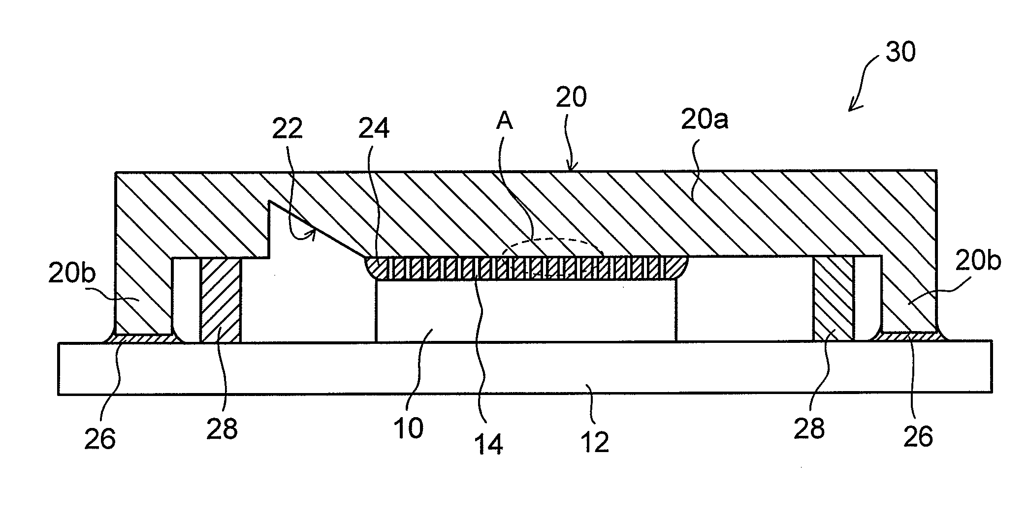
[0028]FIGS. 1A and 1B show the configuration of a semiconductor device (electronic component device) using a thermal interface material according to an embodiment of the present invention. FIG. 1A shows a sectional structure thereof, and FIG. 1B shows an enlarged sectional structure of the part A in FIG. 1A.

[0029]In a semiconductor device 30 of this embodiment, reference numeral 10 denotes a semiconductor element (chip) serving as an electronic component from which heat should be released. The semiconductor element (chip) 10 is mounted on a wiring board (package) 12 with a face surface (the surface on the side where circuits are formed) of the chip 10 facing downward. Although the specific illustration of a connection portion between the wiring board 12 and the chip 10 is omitted, the configuration of this portion is the same as a normal configur...


PUM

PropertyMeasurementUnit
Thicknessaaaaaaaaaa
Electrical conductoraaaaaaaaaa
Areaaaaaaaaaaa

Abstract

A recessed portion is formed in a predetermined position in a heat-spreading component. A thermoplastic resin serving as a thermal interface material (TIM) is stored in the recessed portion. Meanwhile, a large number of filamentous thermo-conductive elements serving as the TIM are arranged to stand side by side on a surface of the heat-spreading component in which the recessed portion is formed (or on an exposed surface of an electronic component). Then, the heat-spreading component is fixed onto a board in such a manner that the surface of the heat-spreading component in which the recessed portion is formed faces the board and that a clearance is adjusted between the electronic component and the heat-spreading component. Thereafter, the resin is heated to a softening point thereof into a fluidized state, and the resin is flowed and filled into the clearance between the electronic component and the heat-spreading component.

Description

CROSS-REFERENCE TO RELATED APPLICATIONS[0001]This application is based on and claims priority of Japanese Patent Application No. 2009-129916 filed on May 29, 2009, the entire contents of which are incorporated herein by reference.BACKGROUND OF THE INVENTION[0002](a) Field of the Invention[0003]The present invention relates to a method of manufacturing an electronic component device. More specifically, it relates to a method of manufacturing an electronic component device including an electronic component such as a semiconductor element mounted on a board, and a heat-spreading component which dissipates to the air, heat generated from the electronic component, and which is coupled via a thermal interface material to the electronic component.[0004](b) Description of the Related Art[0005]A semiconductor element (chip) used in a microprocessor unit (MPU) and the like is electrically connected to and fixed on a wiring board (package) (for example, by flip chip mounting). The semiconducto...

Claims


Application Information

Patent Timeline
IPC IPC(8): H01L21/58
CPCH01L23/3675Y10T29/4913H01L23/3733H01L23/42H01L24/29H01L24/32H01L2924/01005H01L2924/01029H01L2924/01049H01L2924/01075H01L2924/01078H01L2924/01079H01L2224/29H01L2224/2919H01L2224/29298H01L2924/01006H01L2924/01033H01L2924/014H01L2924/0665H01L2224/29101H01L23/373Y10T29/49146Y10T29/49144H01L2924/10253H01L2924/00013H01L2924/00H01L2924/00014H01L2224/29099H01L2224/29199H01L2224/29299H01L2224/2929H01L2224/26175H01L2224/29499H01L2924/15747H01L2924/15788H01L2924/181
Inventor ODA, TAKUYA
Owner SHINKO ELECTRIC IND CO LTD
Why Eureka
Try Eureka