Semiconductor device having additional functional element and method of manufacturing thereof

a technology of semiconductor devices and functional elements, which is applied in the direction of semiconductor devices, semiconductor/solid-state device details, electrical apparatus, etc., can solve the problems of increasing processing speed, reducing voltage, and arranging components highly intensively, so as to reduce the intensity of switching noise, increase processing speed, and reduce operation voltage

Active Publication Date: 2006-02-28
SHINKO ELECTRIC IND CO LTD
View PDF13 Cites 25 Cited by
  • Summary
  • Abstract
  • Description
  • Claims
  • Application Information

AI Technical Summary

Benefits of technology

[0012]It is an object of the present invention to provide a semiconductor device having an additional functional element characterized in that: the conventional semiconductor package can be used as it is; an additional functional element, such as a capacitor, can be arranged at the closest position to a semiconductor element; and an intensity of switching noise can be reduced to as low as possible under the conditions of increasing the processing speed, arranging the components highly intensively and reducing the operation voltage.

Problems solved by technology

However, there is a demand for increasing the processing speed, arranging the components highly intensively and reducing the voltage.
In response to this demand, it has become a serious problem to take countermeasures to reduce the switching noise.
However, when the capacitor is incorporated into the package closer to the semiconductor element, the package manufacturing process becomes complicated and the manufacturing cost is inevitably raised.
However, in this structure, a semiconductor element, that is, an LSI chip is not directly mounted on an alumina ceramic material which is a package.
Therefore, a conventionally used package cannot be used as it is.
However, only one face of the thin film condenser is connected to the semiconductor element, and the other face of the thin film condenser is not connected to the package.
Therefore, a region of the package cannot be effectively used.
Although clearance between both the substrates can be ensured, a sufficiently effective countermeasure can not be taken for reducing switching noise.

Method used


Image

  • Semiconductor device having additional functional element and method of manufacturing thereof
  • Semiconductor device having additional functional element and method of manufacturing thereof
  • Semiconductor device having additional functional element and method of manufacturing thereof

Examples


Embodiment Construction

[0022]Referring to the accompanying drawings, an embodiment of the present invention will be explained in detail as follows.

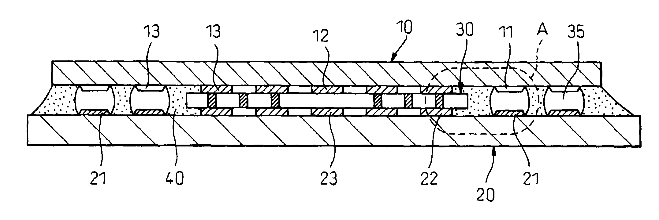
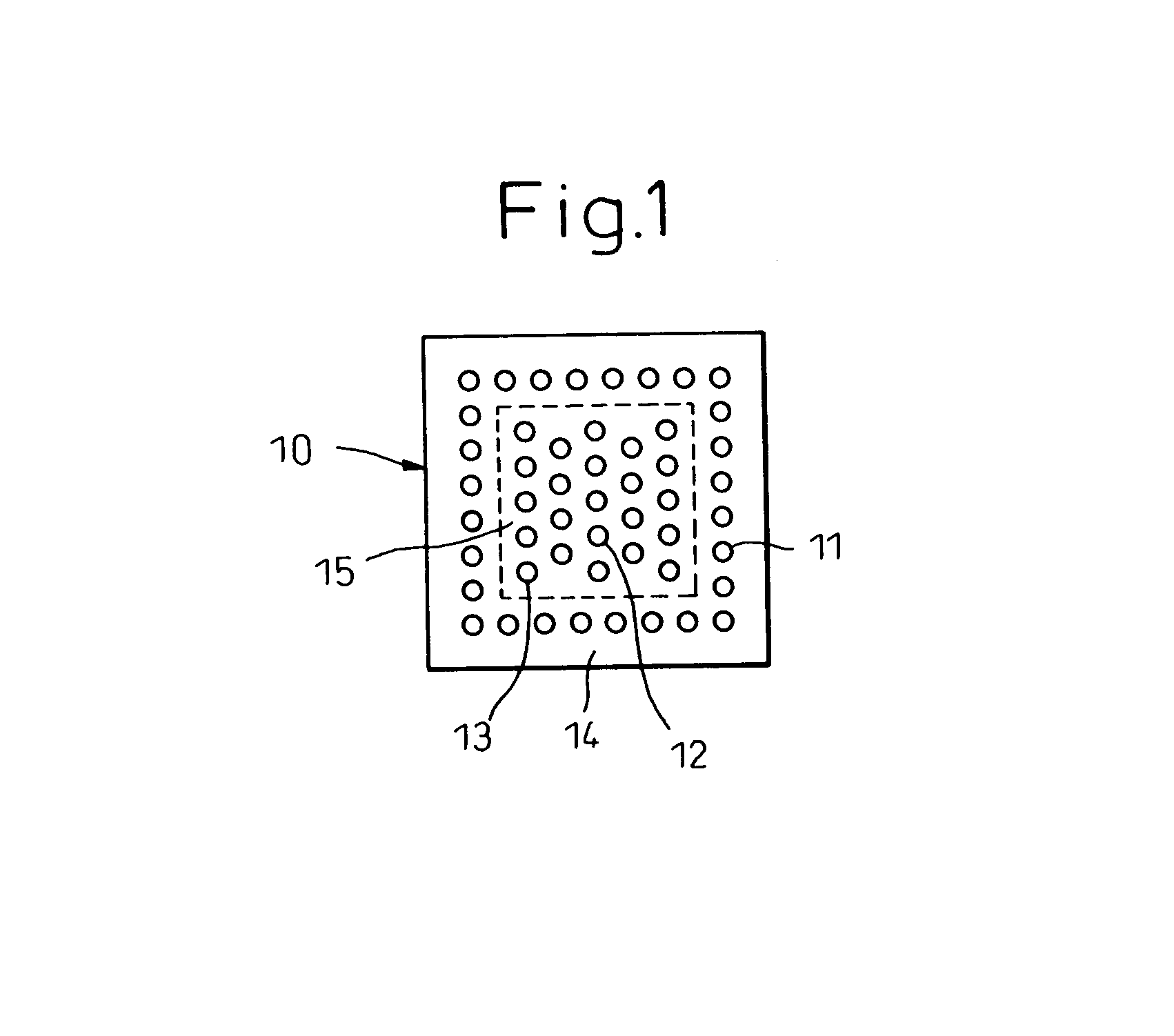
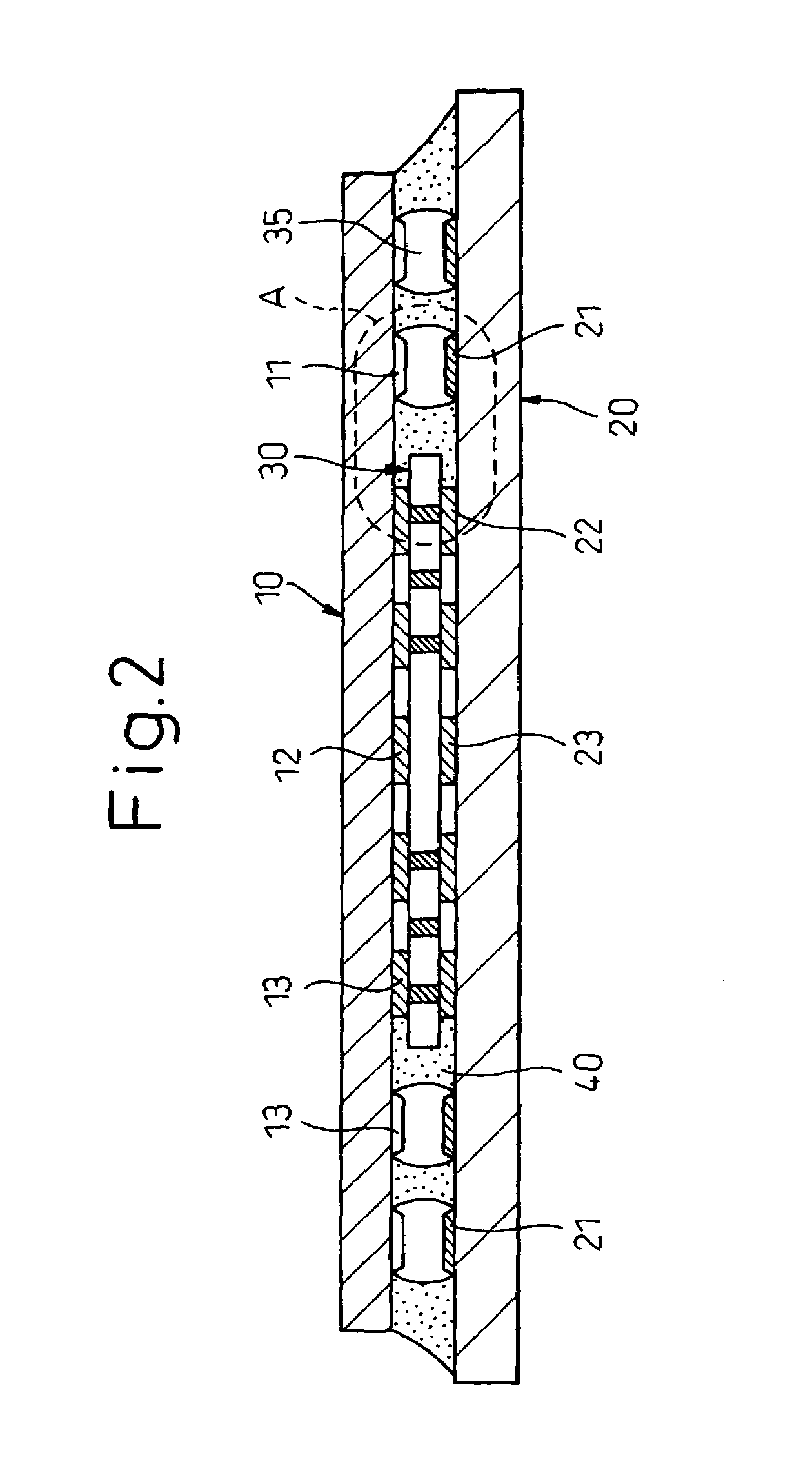
[0023]The semiconductor element or the chip 10 is of the area array type which is mounted by means of flip-chip mounting. Usually, as shown in FIG. 1, a large number of electrodes 11, 12, 13 are arranged like an array on the side on which the electrodes are formed. In the outer peripheral region 14 of the substantially square electrode forming face, the electrodes (the first electrodes) 11 for signal use are arranged. In the inner region of the outer peripheral region or in the central region 15, the electrodes (the second electrodes) 12, which are connected with an upper face of the capacitor 30 of an extremely thin type additional functional element described later, are arranged, and the electrodes (the third and the fourth electrodes) used for electric power supply / ground are also arranged. In each electrode 11, 12, 13, usually, the solder bump 35 used for f...


PUM


Abstract

A capacitor is arranged at the closest position to a semiconductor element and the generation of switching noise is reduced as low as possible by increasing the processing speed, arranging the components highly intensively and reducing the operation voltage. One face of the capacitor is connected to an electrode of the electrode forming face of the semiconductor element and the other face of the capacitor is connected to the connection pads on the wiring board so that the capacitor is interposed between the electrode forming face of the semiconductor element and the semiconductor mounting face of the wiring board, the other face of the capacitor is connected to the connection pads on the wiring board, and at the same time, flip-chip connection is conducted on the connection pads on the wiring board via the solder bumps connected to the electrodes of the semiconductor element.

Description

BACKGROUND OF THE INVENTION[0001]1. Field of the Invention[0002]The present invention relates to a semiconductor device into which a passive element or an active element, to exhibit a specific electric functional such as a capacitor, resistor, inductance or the like, which will be referred to as an “additional functional element” hereinafter, is incorporated. The present invention also relates to a method of manufacturing such a semiconductor device.[0003]2. Description of the Related Art[0004]In the case of a semiconductor device such as MPU (micro processing unit), CPU (central processing unit) or the like having a large number of transistors, in which the electric power sources of these transistors are simultaneously switched, that is, these transistors are simultaneously turned on and off, a high intensity of electric current flows between the electric power source and the ground when the transistors are switched. Therefore, voltage fluctuates, that is, what is called “simultane...

Claims


Application Information

Patent Timeline
Patent Type & Authority Patents(United States)
IPC IPC(8): H01L29/40H01L25/00H01L21/56H01L21/822H01L23/64H01L27/04
CPCH01L21/563H01L23/642H01L24/73H01L2924/07811H01L2224/16H01L2224/73203H01L2924/01004H01L2924/01029H01L2924/01082H01L2924/14H01L2924/19041H01L2924/19103H01L2924/30107H01L2924/3011H01L2924/01006H01L2924/01033H01L2924/00H01L2924/15787H01L2224/05573H01L2224/05568H01L2924/00014H01L2224/06051H01L2924/19104H01L2224/16227H01L2224/16265H01L2224/05599
Inventor KOIZUMI, NAOYUKI
Owner SHINKO ELECTRIC IND CO LTD
Why Eureka
Try Eureka