
Eureka
For R&D, Eureka makes reading and utilizing patents & technical documents easy.
Eureka AIR
Designed for self-driven R&D workflows. Generate viable solutions, solve complex R&D challenges, empower your innovation with AI.

Eureka Materials
Designed for material experts only. Revolutionize your material R&D, from search, analyze, to developing new materials.

TechResearch
Generate reliable direction feasibility study reports for your R&D in just a few steps.

TechSeek
Discover and master advanced knowledge NOW. Basics, ideas, possibilities, all at once.

TechMind
As an expert in R&D Theories, TechMind can generates customized viable solutions instantly.

TechRisk
Analyze your overall solution with one click, know your potential R&D risks in advance.

TechMonitor
Get weekly tech updates, stay abreast of the latest tech innovations and key insights.
Light-emitting material and light-emitting element
- Summary
- Abstract
- Description
- Claims
- Application Information
AI Technical Summary
Benefits of technology
Problems solved by technology
Method used
Image

Examples
example 1
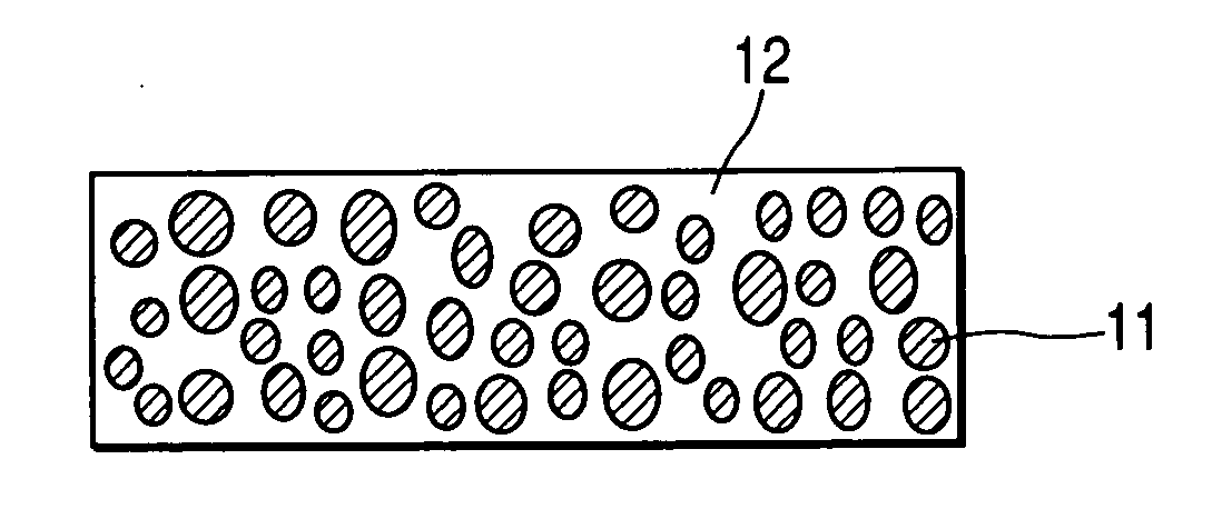
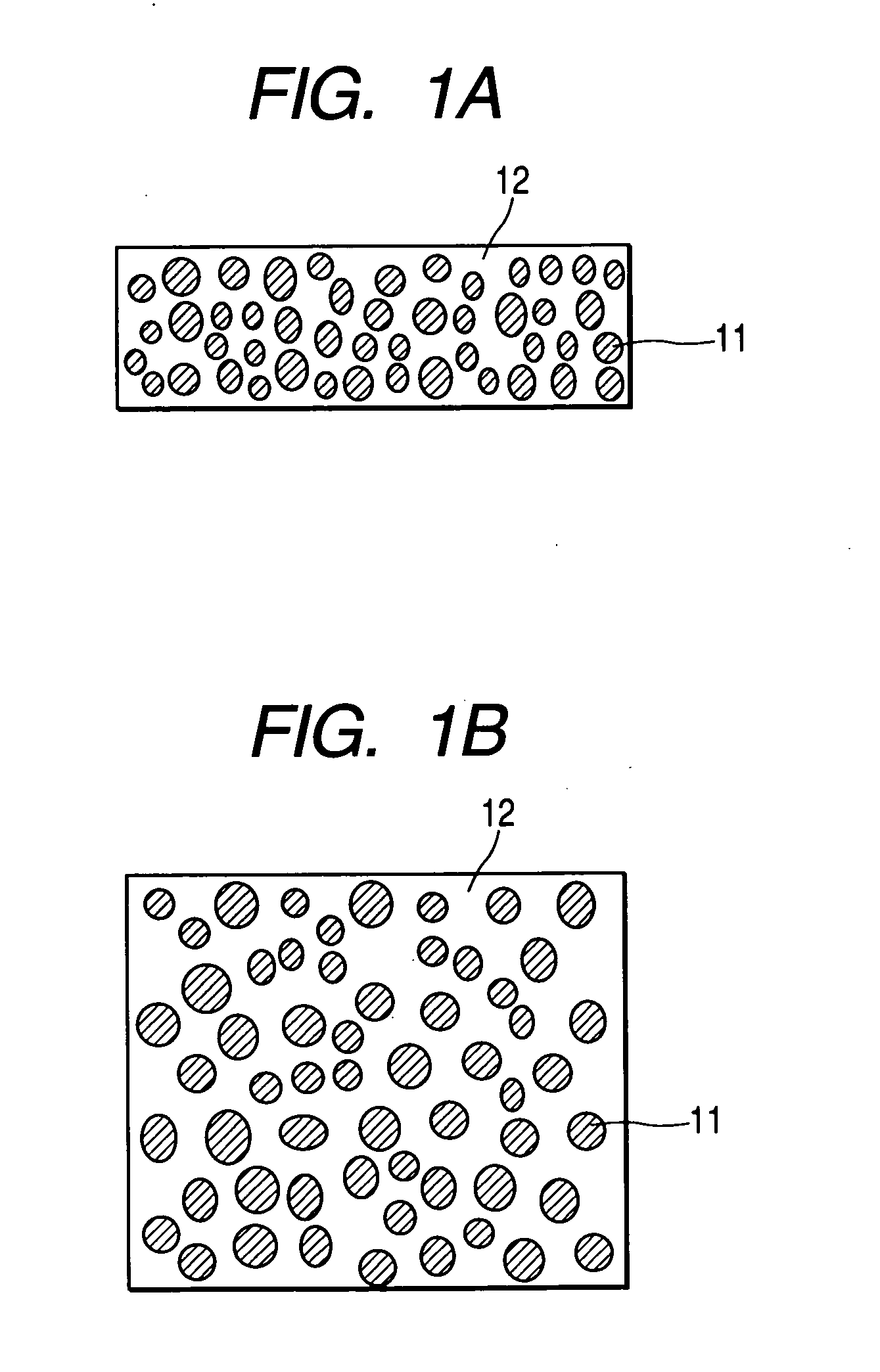
[0060] An embodiment of light-emitting material according to the invention will also be described here by referring to FIGS. 1A, 1B and 4A.
[0061] A quartz substrate is used as substrate in this example. An electrode film 45 is formed by depositing Ti and Au to respective thicknesses of 10 nm and 50 nm on a substrate 46 by magnetron sputtering. Subsequently, a dielectric film 44 is formed by depositing BaTiO3 to a thickness of 2 μm also by magnetron sputtering. Thereafter, a phosphor film 43 is formed in a manner as described below.
[0062] A target with a composition showing a volume ratio of MgO to Y2O3:Eu equal to 2 to 1 is prepared. A phosphor film 43 of MgO+Y2O3:Eu is formed to a thickness of 5 μm by magnetron sputtering, using the target. The substrate temperature is varied from the room temperature to 1,000° C. during the sputtering process. Then, a dielectric film 42 of BaTiO3 is formed to a thickness of 2 μm and subsequently a transparent electrically conductive film 41 of I...
example 3
[0071] A light-emitting material of a V2O5—Y2O3 system is prepared in this example by using a technique similar to the one used in Example 1.
[0072] A quartz substrate is used as substrate in this example. An electrode film 45 is formed by depositing Ti and Pt to respective thicknesses of 10 nm and 50 nm on a substrate 46 by magnetron sputtering. Subsequently, a dielectric film 44 is formed by depositing Ta2O5 to a thickness of 0.5 μm also by magnetron sputtering. Thereafter, a phosphor film 43 is formed in a manner as described below.
[0073] A target with a composition showing a volume ratio of V2O5 to Y2O3:Eu equal to 5 to 1 is prepared. A phosphor film 43 of V2O5+Y2O3:Eu is formed to a thickness of 1 μm by magnetron sputtering, using the target. The substrate temperature is varied from the room temperature to 1,000° C. during the sputtering process. Then, a dielectric film 42 of BaTiO3 is formed to a thickness of 2 μm and subsequently a transparent electrically conductive film 41...
example 4
[0076] In this example, as shown in FIG. 6, a light-emitting material according to the invention is used as a phosphor thin film for exciting electron beams.
[0077] A transparent electrically conductive film 63 of SnO2:F is formed to a thickness of 300 nm on a glass substrate 64 and then NiO and Y2O3:Eu are deposited thereon to form a film to a thickness of 2 μm by sputtering. NiO and Y2O3:Eu are made to show a ratio of 2:1 in order to form a phosphor film 62. Then, Al is deposited thereon to form an electrode film 61 to a thickness of 50 nm.
[0078] The prepared product is put into a vacuum chamber and irradiated with electron beams to evaluate the phosphor. As a result, it is found that it emits red light. As a result of comparing a known ordinary Y2O3:Eu thin film and the phosphor thin film, the ordinary phosphor film with no electrode film 61 is easily charged up, while the phosphor film of the present invention with no electrode film 61 is charged up only very slightly.
PUM
| Property | Measurement | Unit |
|---|---|---|
| Dielectric polarization enthalpy | aaaaa | aaaaa |
Abstract
Description
Claims
Application Information
 - R&D Engineer
- R&D Manager
- IP Professional
- Industry Leading Data Capabilities
- Powerful AI technology
- Patent DNA Extraction
Browse by: Latest US Patents, China's latest patents, Technical Efficacy Thesaurus, Application Domain, Technology Topic, Popular Technical Reports.
© 2024 PatSnap. All rights reserved.Legal|Privacy policy|Modern Slavery Act Transparency Statement|Sitemap|About US| Contact US: help@patsnap.com