Wiring carrier design

a wiring carrier and carrier technology, applied in the direction of electrical equipment, semiconductor devices, semiconductor/solid-state device details, etc., can solve the problems of affecting the quality of the adhesive connection of the chip on the wiring carrier, the stencil is partly or entirely pressed, and the plane bearing area is no longer available for all parts of the stencil, so as to achieve uniform adhesive application

Inactive Publication Date: 2005-10-06
INFINEON TECH AG
View PDF6 Cites 1 Cited by
  • Summary
  • Abstract
  • Description
  • Claims
  • Application Information

AI Technical Summary

Benefits of technology

[0008] In one aspect, the invention provides a wiring carrier design ...

Problems solved by technology

This has the consequence, however, that a closed and plane bearing area is no longer available for all parts of the stencil.
The resultant disadvantage is that, due to the forces acting during the printing operation, parts of the stencil are partly or else entirely pressed onto the carrier material.
The fact that the layer of adhesive thus has varying th...

Method used


Image

  • Wiring carrier design
  • Wiring carrier design

Examples


Embodiment Construction

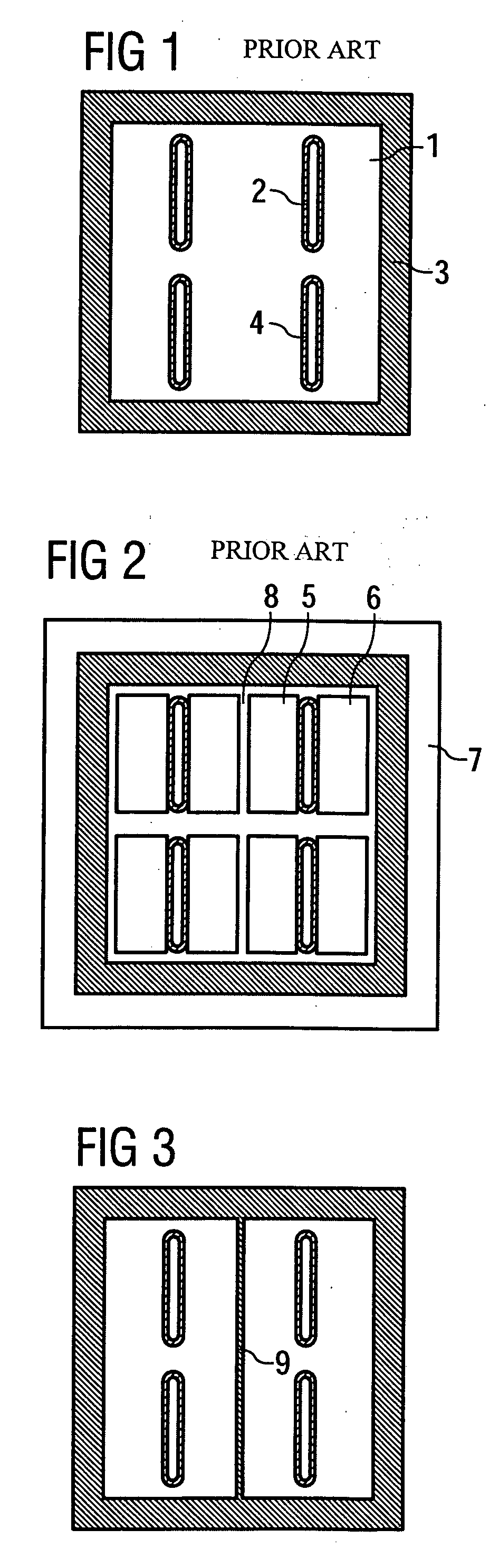
[0028]FIG. 1 shows a customary wiring carrier 1 according to the prior art, which is provided with bonding channels 2 and a soldering resist layer 4 around the bonding channels 2 and also a further soldering resist layer 3 on the edge of the wiring carrier 1.

[0029]FIG. 2 shows the same wiring carrier according to FIG. 1 with a printing stencil 7 laid thereon and the openings 6 thereof in the printing stencil 7 for the application of adhesive to the wiring carrier.

[0030] The opening 6 in the printing stencil 7 bears closely on the soldering resist on three sides (on the left, at the top and on the right in accordance with the drawing), the web in the stencil on the bottom side being wide and scarcely compliant. The layer of adhesive applied through the opening 6 in the printing stencil 7 thus has a uniform layer thickness corresponding to the sum of the thicknesses of stencil and soldering resist.

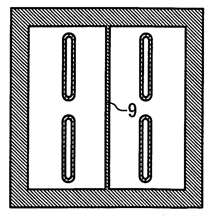
[0031] The opening 5 in the printing stencil bears closely on the soldering resist on...


PUM


Abstract

The invention relates to a wiring carrier design for a planar wiring carrier for receiving a plurality of chips, on the chip side of which chips of identical type are arranged in matrix-like fashion, a long narrow bonding channel surrounded by a soldering resist layer being situated in the center of each chip receptacle, and the further region of the chip receptacle area being free of soldering resist, and the chips in each case being encapsulated with a molding material. The invention is based on the object of providing a wiring carrier design with which a uniform application of adhesive can be achieved using simple means. The object is achieved by virtue of the fact that additional supporting elements (9) made of soldering resist, or made of some other suitable material, are applied on the wiring carrier (1) at least in the region of narrow stencil webs (8) that are readily flexible during the printing operation.

Description

[0001] This application claims priority to German Patent Application 10 2004 015 091.5, which was filed Mar. 25, 2004 and is incorporated herein by reference. TECHNICAL FIELD [0002] The invention relates to a wiring carrier design for a planar wiring carrier for receiving a plurality of chips. BACKGROUND [0003] Wiring carriers of this type comprise a carrier material, on the chip side of which a cured layer of a soldering resist has been applied essentially over the whole area. For fixing the chips, an adhesive layer is applied on the soldering resist on the envisaged mounting position of the chip. This may be effected by means of customary methods appertaining to printing technology, e.g., the stencil printing method. The adhesive is consequently cured, e.g., by means of a heat treatment process. [0004] A stencil is used for the application of adhesive, which stencil finds a closed and plane bearing area on the soldering resist. As a result, the applied layer of adhesive has a thic...

Claims


Application Information

Patent Timeline
IPC IPC(8): H01L21/48H01L21/58H01L21/60H01L23/13H01L23/495
CPCH01L21/4867H01L2224/83136H01L2224/2732H01L2224/83801H01L24/27H01L2224/83192
Inventor UHLMANN, RUEDIGER
Owner INFINEON TECH AG
Why Eureka
Try Eureka