Capacitive-load driving circuit capable of properly handling temperature rise and plasma display apparatus using the same

a technology of driving circuit and temperature rise, which is applied in the direction of instruments, television systems, and electrodes, etc., can solve the problems of increasing component cost, reducing power consumption reduction design effectiveness, and reducing the effect of power consumption reduction design

Inactive Publication Date: 2005-10-06
FUJITSU HITACHI PLASMA DISPLAY LTD
View PDF30 Cites 8 Cited by
  • Summary
  • Abstract
  • Description
  • Claims
  • Application Information

AI Technical Summary

Benefits of technology

[0014] The power distributing circuit may be a resistive element having an impedance whose value is not smaller than one-tenth of the value of a resistive component of the conducting impedance of the driving device. The power distributing circuit may be a high-power resistor having a capability to handle power higher than the allowable power of the driving device. The power distributing circuit may be a constant-current source.
[0015] The driving power supply source may output a plurality of different voltage levels in a selective manner. The power distributing circuit may include a plurality of power distributing units, one for each of the plurality of different voltage levels. Each of the power distributing units may have a function as a switch for selecting one of the plurality of different voltage levels. The driving device may be a device whose input withstand voltage is higher than an output voltage.

Problems solved by technology

The prior art capacitive-load driving circuit recovers power by utilizing a phenomenon of resonance, but with the recent trend toward higher-resolution and larger-screen plasma display panels, the power consumption reduction design has been losing its effectiveness significantly.
If the power consumption of the driving circuit cannot be reduced sufficiently, the cost involved in removing heat from various parts of the display, and therefore, the component cost, increases, and besides, this could lead to a situation where the display brightness is reduced due to the limit of the heat dissipation capability of the display apparatus itself, or where the advantage of the flat panel display, i.e., thin and light-weight construction, cannot be exploited to the full.
Furthermore, as the output frequency of the driving circuit increases, power consumption increases due to the generation of high-voltage pulses to drive the plasma display panel, and a temperature rise in the driving circuit (drive IC) becomes a serious concern.

Method used


Image

  • Capacitive-load driving circuit capable of properly handling temperature rise and plasma display apparatus using the same
  • Capacitive-load driving circuit capable of properly handling temperature rise and plasma display apparatus using the same
  • Capacitive-load driving circuit capable of properly handling temperature rise and plasma display apparatus using the same

Examples


first embodiment

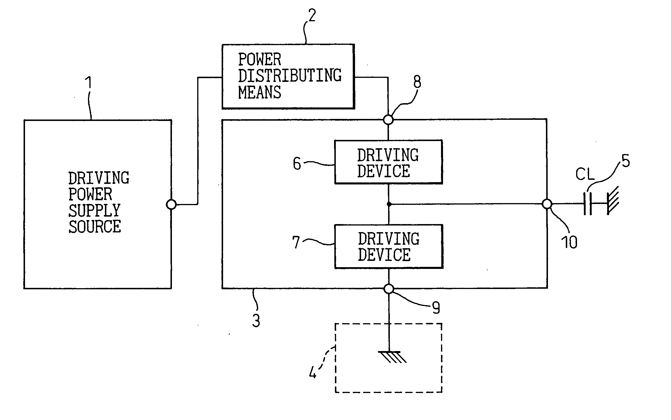
[0080]FIG. 4 is a block diagram showing the capacitive-load driving circuit according to the present invention. In FIG. 4, reference numeral 1 is a driving power supply source, 21 is a power distributing means, 3 is an address drive IC, 4 is a reference potential point (ground point), 5 is a load capacitor, 6 and 7 are driving devices, 8 and 9 are a power supply terminal and a reference potential terminal (ground terminal), respectively, of the address drive IC, and 10 is an output terminal of the address drive IC.

[0081] As shown in FIG. 4, in the first embodiment, the power distributing means 21 is inserted between the driving power supply source 1 and the high-level voltage supply terminal 8 of the address drive IC 3; this power distributing means is constructed as a resistive impedance (resistive element) 21 whose value is higher than about one-tenth of the resistive impedance that the driving device 6 provides at the time of conduction (the resistive component of the conducting ...

second embodiment

[0083]FIG. 5 is a block diagram showing the capacitive-load driving circuit according to the present invention.

[0084] As shown in FIG. 5, in the second embodiment, the power distributing means in the foregoing first embodiment is constructed as a constant-current source 22. With the driving circuit of the second embodiment, the effective value of the current flowing in the driving device 6 can be made the smallest under the same driving conditions; as a result, theoretically, the power consumption of the driving circuit 3 can be reduced to the lowest value.

[0085]FIG. 6 is a circuit diagram showing one example of the constant-current source in the capacitive-load driving circuit shown in FIG. 5.

[0086] As shown in FIG. 6, the constant-current source 22 comprises an n-channel MOS transistor (nMOS transistor) 221 whose gate-to-source voltage is biased, for example, to a constant voltage by a Zener diode 222. As shown, a resistor 225 may be connected in series to the source of the tran...

fourth embodiment

[0091]FIG. 9 is a block diagram showing the capacitive-load driving circuit according to the present invention.

[0092] In the fourth embodiment, the switches 12, 13, and 14 in the driving power supply source 1 of FIG. 7 described above are replaced by nMOS transistors 121, 131 / 132, and 141, respectively, whose gate voltages are controlled by a driving power control circuit 15, thus making the driving power supply source 1 also perform the function of the power distributing means using the constant-current sources as in the second embodiment shown in FIG. 5. In the fourth embodiment, diodes 130 and 1301 are connected in series to the drains of the transistors 131 and 132 but, instead, these diodes may be inserted in series to the sources of the transistors 131 and 132. Further, in FIG. 9, the switches in the driving power supply source 1 are constructed from nMOS transistors, but it will be appreciated that use can also be made of other active devices such as pMOS transistors or bipol...


PUM


Abstract

A capacitive-load driving circuit has a configuration in which a driving power supply source is connected to an output terminal via a driving device. The capacitive-load driving circuit has a power distributing circuit inserted between the driving power supply source and the driving device. Therefore, temperature rise (power consumption) in the capacitive-load driving circuit can be distributed.

Description

CROSS-REFERENCE TO RELATED APPLICATIONS [0001] This application is a Divisional of application Ser. No. 09 / 933,166, filed Aug. 21, 2001, now pending, and claims the benefit of Japanese Application Nos. 2000-393510, filed Dec. 25, 2000 and 2000-301015, filed Sep. 29, 2000 in the Japanese Patent Office.BACKGROUND OF THE INVENTION [0002] 1. Field of the Invention [0003] The present invention relates to a capacitive-load driving circuit and a plasma display apparatus using the same, and more particularly, to a circuit technique capable of properly handling the temperature rise occurring due to the driving of capacitive loads in a plasma display panel, an electronic luminescence panel, and the like. [0004] 2. Description of the Related Art [0005] Recently, a variety of display apparatuses have been researched and developed, and the research and development of thin flat display apparatuses, exemplified by plasma display panels (PDP) and electronic luminescence (EL) panels, has been procee...

Claims


Application Information

Patent Timeline
Patent Type & Authority Applications(United States)
IPC IPC(8): G09G3/20H04N5/66G09G3/282G09G3/288G09G3/296G09G3/298H01J11/26H05B44/00
CPCG09G3/28G09G3/296G09G3/2965G09G2310/0289H01J11/26G09G2330/021G09G2330/045H05B33/08G09G2330/02H05B44/00
Inventor SANO, YUJITAKAGI, AKIHIROKISHI, TOMOKATSUKAWADA, TOYOSHIINOUE, HIROKAZU
Owner FUJITSU HITACHI PLASMA DISPLAY LTD
Why Eureka
Try Eureka