

Differential stage voltage offset trim circuitry
- Summary
- Abstract
- Description
- Claims
- Application Information
AI Technical Summary
Benefits of technology
Problems solved by technology
Method used
Image

Examples
Embodiment Construction
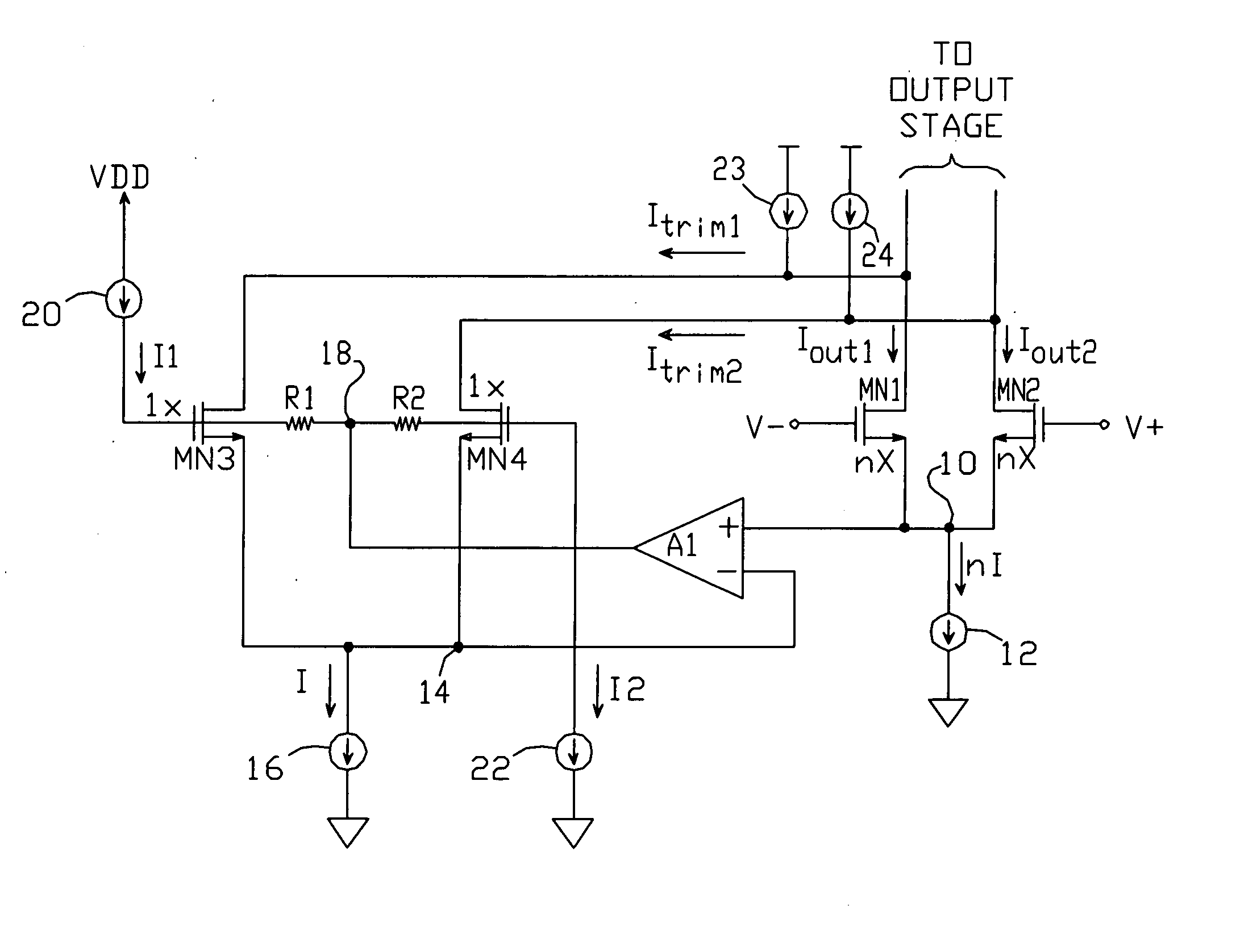
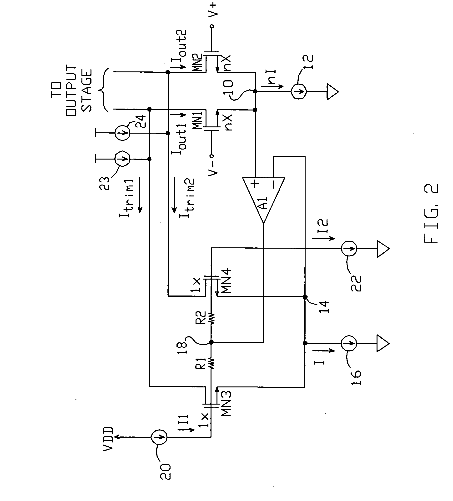
[0023] The present invention provides several trim circuits, each of which addresses one particular source of offset voltage error for a differential stage. When used in combination, the stage's voltage offset error is substantially reduced.
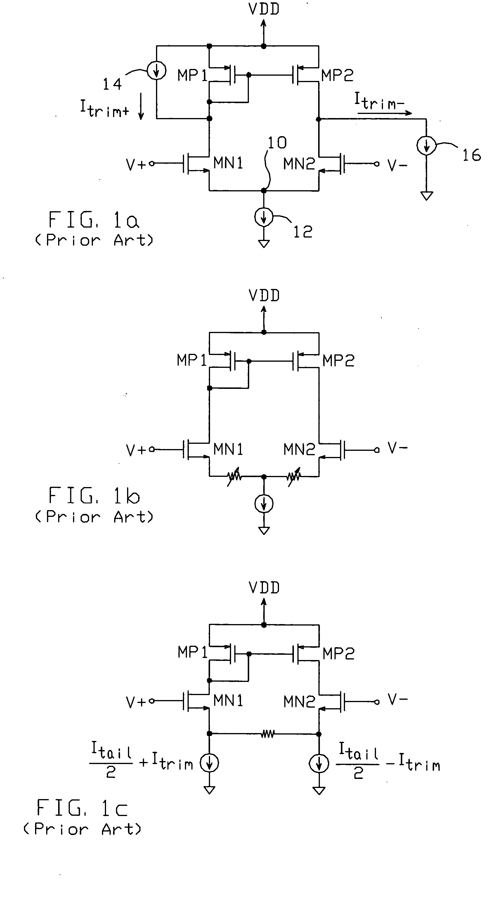
[0024] The circuits described herein are applicable to both bipolar and FET differential stages, whether they are input or non-input stages. The invention is also applicable to the active loads of differential stages. Rail-to-rail amplifiers are also contemplated, as the invention could be used to reduce offset voltage error associated with both the p-type and n-type differential pair. However, for purposes of the present discussion, a single FET differential input stage is used to illustrate the invention's operation.
[0025] The most common source of voltage offset error in a FET differential input stage arises due to a mismatch between the threshold voltages of the transistors making up the “main” differential pair—i.e., the pair whose offset ...
PUM
 Abstract
Description
Claims
Application Information