

Photomask features with chromeless nonprinting phase shifting window
a technology of phase shifting window and photomask, which is applied in the field of chromeless nonprinting phase shifting window of photomask features, can solve the problems of reducing the resolution of the image,
- Summary
- Abstract
- Description
- Claims
- Application Information
AI Technical Summary
Benefits of technology
Problems solved by technology
Method used
Image

Examples
Embodiment Construction
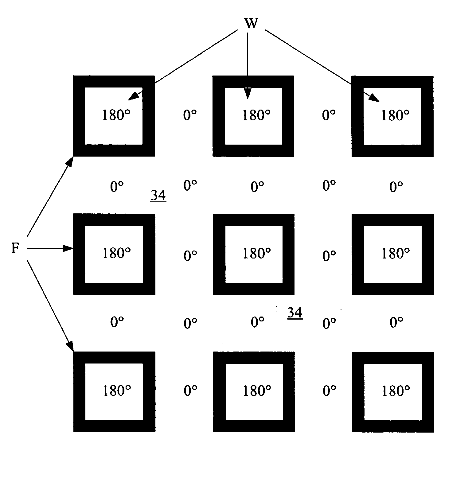
[0043] One approach to allow alternating phase shifting photomasks to be used to pattern a wider variety of shapes is taught in Chen, U.S. patent application Ser. No. 10 / 728,436, filed Dec. 5, 2003, hereinafter the '436 application. The '436 application is the work of the same inventor as the present invention, is owned by the assignee of the present invention, and is hereby incorporated by reference. The present invention is an improved method to solve the same problem.
[0044] The problem addressed by both the present invention and the '436 application will be described.
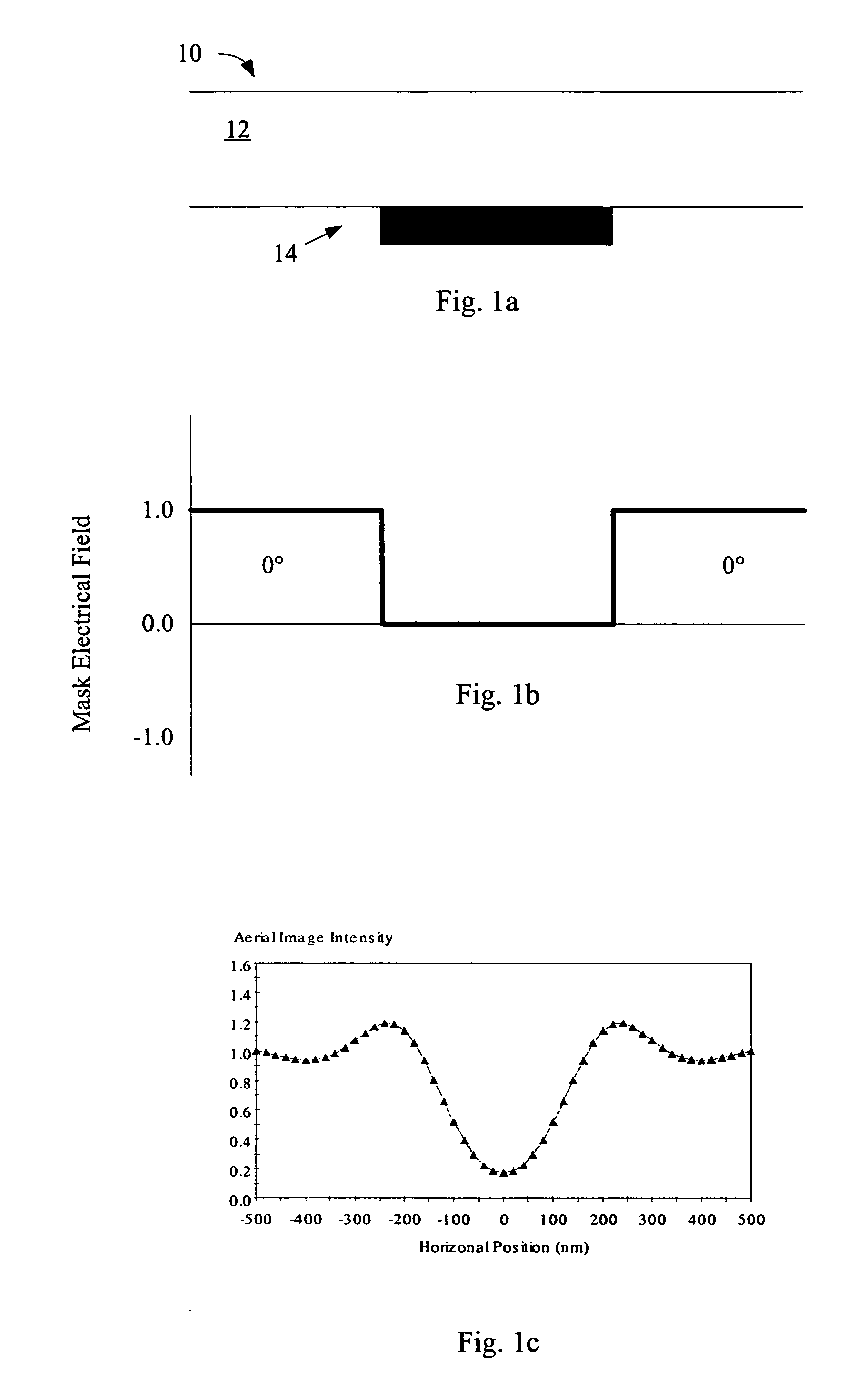
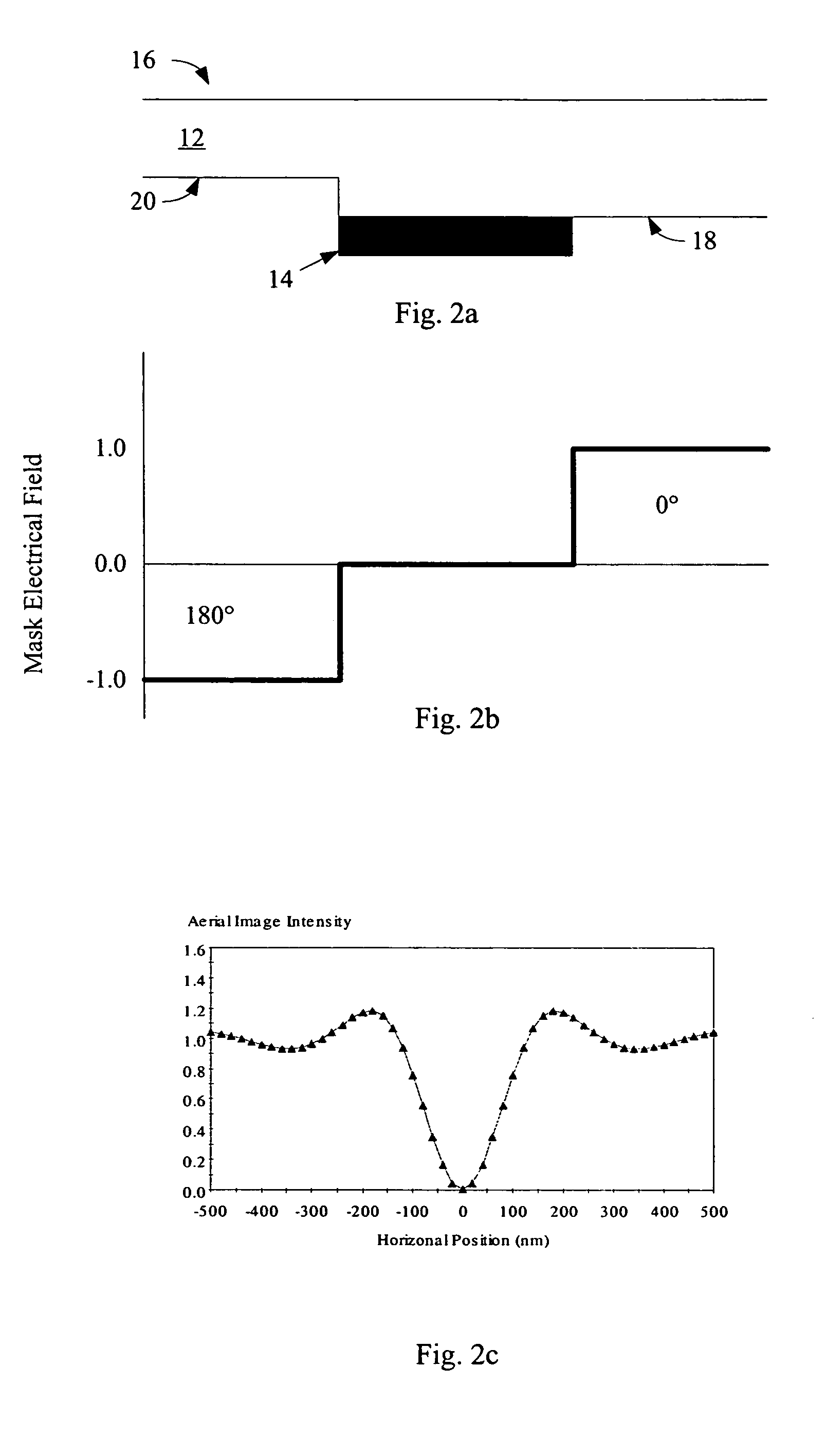
[0045] The '436 application used the term maskedfeature. A masked feature referred to a feature in a photomask, for example a line, a rectangle, or any other shape. A masked feature in a photomask substantially entirely or partially obscures light, so that when light is projected through the photomask, a corresponding feature in the photoresist is shielded from light, while the area outside of the obscured area is ...
PUM
 Abstract
Description
Claims
Application Information