Method of manufacturing a semiconductor device and a method for fixing the semiconductor device using substrate jig

a technology of semiconductor devices and substrates, which is applied in the direction of manufacturing tools, lapping machines, other domestic objects, etc., can solve the problems of failure of the back grinding step, failure of the appropriate process in the steps subsequently conducted, and the performance of each manufacturing step after the back grinding step is degraded, so as to suppress the occurrence of damage

Inactive Publication Date: 2005-10-06
SOCIONEXT INC
View PDF8 Cites 8 Cited by
  • Summary
  • Abstract
  • Description
  • Claims
  • Application Information

AI Technical Summary

Benefits of technology

[0019] In view of the above problems, the general object of the present invention is to provide a jig for holding the semiconductor substrate so that there is little effect from thinned semiconductor substrates, and for suppressing the occurrence of damage caused by lack of semiconductor substrate strength; and to provide a method of manufacturing a semiconductor device using the jig.

Problems solved by technology

When the wafer 1 warps, the performance of each manufacturing step after the back grind step is degraded, and along with transportation of the wafer becomes a factor of breakage failure.
Therefore, when bubbles enter, there is a possibility that an appropriate process may not be successfully performed in the steps subsequently conducted (for example, the singularization step), and the yield of the semiconductor manufacturing process is lowered, and in the worst case, the wafer 1 may break due to the expansion of bubbles.

Method used


Image

  • Method of manufacturing a semiconductor device and a method for fixing the semiconductor device using substrate jig
  • Method of manufacturing a semiconductor device and a method for fixing the semiconductor device using substrate jig
  • Method of manufacturing a semiconductor device and a method for fixing the semiconductor device using substrate jig

Examples


first embodiment

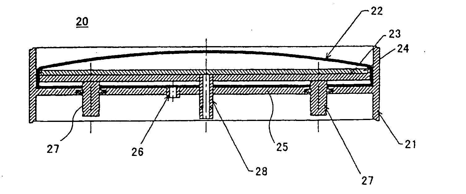
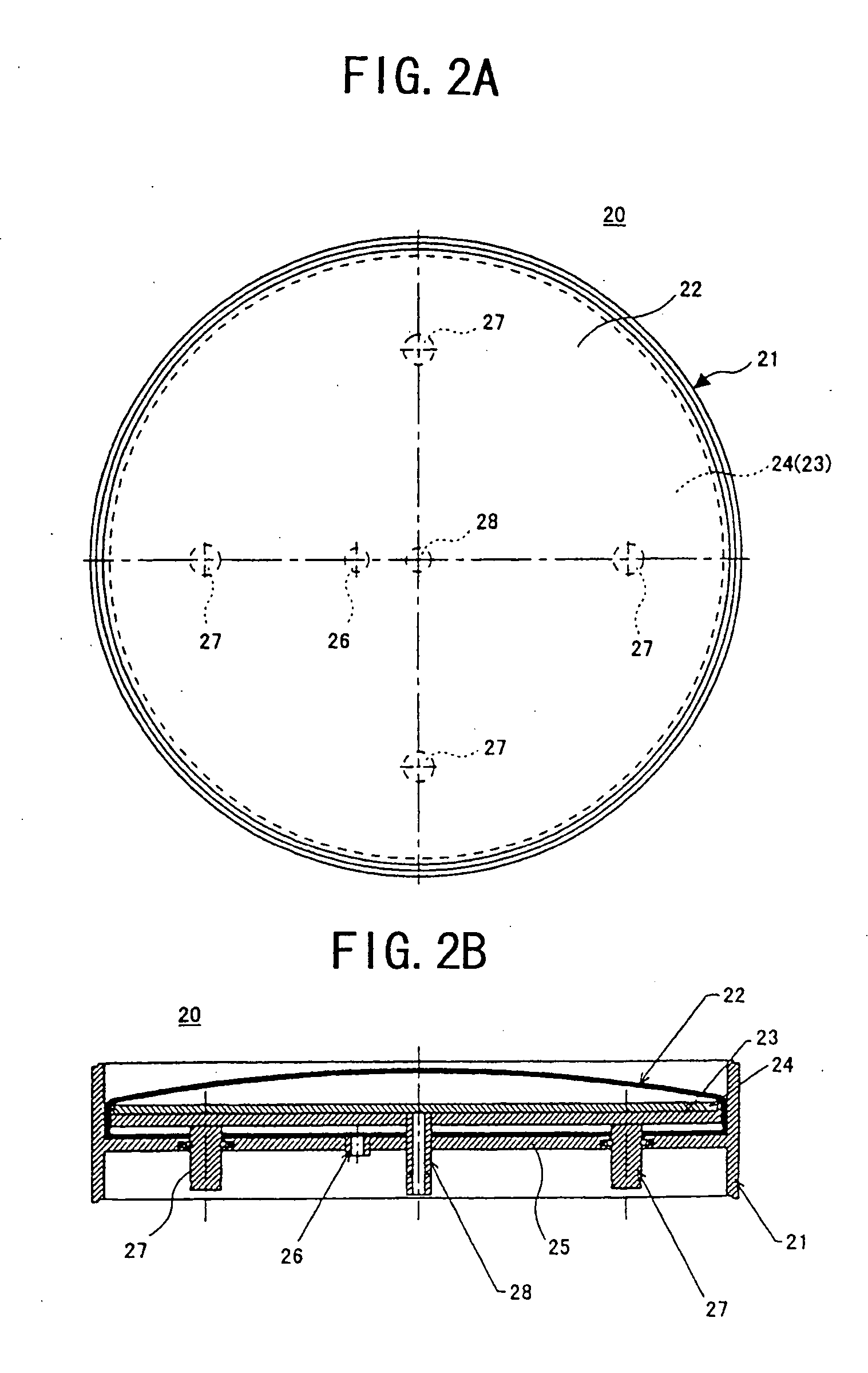
[0120]FIG. 2 shows a wafer-fixing jig 20 according to the present invention. FIG. 2A is a top view of the wafer-fixing jig 20, and FIG. 2B is a cross sectional view of the wafer-fixing jig 20. Components having the same structure as those previously described with reference to FIG. 1 are explained with the same reference numbers.

[0121] The wafer-fixing jig 20 generally includes for example, a rubber film 22, a set table 23, and a porous plate 24. The outer frame 21 is a cylinder shaped member made from metal (ceramic and resin are also possible), and floor 25 is placed in the center (refer to FIG. 2B). The size of the outer frame 21 (diameter when seen from the top) is set to be slightly larger than the external shape of the wafer 1. The rubber film 22 is arranged on the upper part of the floor formed in the wafer-fixing jig 20.

[0122] The rubber film 22 is made elastic by injecting fluids (in this embodiment, air, but, other gases or fluids are also possible) inside. The rubber fil...

second embodiment

[0165] Now, the present invention according to the method of manufacturing a semiconductor device is explained.

[0166]FIG. 6 is a flow diagram of a method of manufacturing a semiconductor device according to a second embodiment. In this embodiment as well, each manufacturing step is performed using the wafer-fixing jig 20 shown in FIG. 2.

[0167] In FIG. 6, components the same as those shown in FIG. 3 through FIG. 5 have the same reference numbers and thus their explanations are omitted. Steps the same as those explained in the first embodiment are omitted to avoid redundancy of the explanation. This holds for each of the subsequent embodiments explained after the second embodiment.

[0168] In this embodiment, the attachment step and the back grind step are carried out in a similar manner as those explained in the first embodiment. This embodiment, however, is characterized in that in the tape reapplication step following the back grind step, a conventionally used frame 5 arranged with...

third embodiment

[0171] Next, a third embodiment according to the method of manufacturing the semiconductor device is explained.

[0172]FIG. 7A through FIG. 7I show flow diagrams of a method of manufacturing the semiconductor device according to a third embodiment. In this embodiment as well, each manufacturing step is performed using the wafer-fixing jig 20 shown in FIG. 2. In this figure, two manufacturing methods in which one flows as FIG. 7A.fwdarw.FIG. 7B.fwdarw.FIG. 7C.fwdarw.FIG. 7D.fwdarw.FIG. 7E.fwdarw.FIG. 7F.fwdarw.FIG. 7G (manufacturing method 1) and the other flows as FIG. 7A.fwdarw.FIG. 7B.fwdarw.FIG. 7C.fwdarw.FIG. 7H.fwdarw.FIG. 7I.fwdarw.FIG. 7G (manufacturing method 2) are shown in the same diagram for convenience.

[0173] In this embodiment, the attachment step and the back grind step are the same as those shown according to the first embodiment (refer to FIG. 3). However, this embodiment is characterized in that in the first embodiment, the tape reapplication step is conducted after...


PUM

PropertyMeasurementUnit
thicknessaaaaaaaaaa
thicknessaaaaaaaaaa
thicknessaaaaaaaaaa

Abstract

The present invention relates to a method of manufacturing a semiconductor substrate including the back grind step, the dicing step, the pick up step, and the die bonding step of the wafer; and to a semiconductor substrate jig used in such method. The object of the present invention is to mitigate the effect and to prevent damage caused by the lack of strength in thinned semiconductor substrates. A jig with an outer frame 21, and a rubber film 22 arranged within the outer frame 21 and having increasing and decreasing body size while deforming its shape by supplying air therein are provided. As the volume of the rubber film 22 increases, the wafer-fixing jig 20 deforms the rubber film and allows the tapes 2 and 6 arranged between the wafer 1 and the rubber film 22A to be pushed toward the wafer 1 gradually from the center outward. The attachment step, the back grind step, the tape reapplication step, the pick up step and the die bonding step are conducted using such wafer-fixing jig.

Description

CROSS REFERENCE TO RELATED APPLICATION [0001] This application is a divisional application of U.S. Ser. No. 10 / 708,067, filed on Feb. 6, 2004 (which is a divisional application of U.S. Ser. No. 10 / 101,169, filed on Mar. 20, 2002), the entire contents of which are incorporated herein by reference.BACKGROUND OF THE INVENTION [0002] This application claims the benefit of a Japanese Patent Application No. 2001-322811 filed Oct. 19, 2001 in the Japanese Patent Office, the disclosure of which is hereby incorporated by reference. [0003] 1. Field of the Invention [0004] The present invention generally relates to jigs for semiconductor substrates and methods for manufacturing semiconductor devices using the same, and more particularly to a method of manufacturing a semiconductor device including a step of back grinding the back surface of the semiconductor substrate (wafer), a step of dicing for singularizing into semiconductor elements, and a step of bonding including picking up such singul...

Claims


Application Information

Patent Timeline
Patent Type & Authority Applications(United States)
IPC IPC(8): H01L21/00H01L21/68H01L21/301H01L21/304H01L21/52H01L21/58H01L21/60H01L21/683H01L21/687
CPCB24B37/042B32B37/003B32B37/1018B32B38/0012B32B2310/0831B32B2457/14H01L21/304H01L21/67092H01L21/67132H01L21/6836H01L21/6838H01L21/78H01L24/27H01L24/83H01L2221/68318H01L2221/68327H01L2221/6834H01L2224/83191H01L2224/8385H01L2924/01004H01L2924/01005H01L2924/01013H01L2924/01029H01L2924/01033H01L2924/01074H01L2924/01075H01L2924/01082H01L2924/07802H01L24/29H01L2924/01006H01L2924/01019H01L2924/01087H01L2924/3512H01L2924/00Y10T29/53191Y10T428/1452Y10T29/5313H01L21/68
Inventor TESHIROGI, KAZUOSHIMOBEPPU, YUZOYOSHIMOTO, KAZUHIROWATANABE, MITSUHISASHINJO, YOSHIAKIYOSHIDA, EIJIHAYASAKA, NOBORU
Owner SOCIONEXT INC
Why Eureka
Try Eureka