Photovoltaic device

Inactive Publication Date: 2005-10-13
BP CORP NORTH AMERICA INC
View PDF2 Cites 56 Cited by
  • Summary
  • Abstract
  • Description
  • Claims
  • Application Information

AI Technical Summary

Problems solved by technology

The continuous challenge in the field of solar energy is to develop and manufacture photovoltaic devices having a high efficiency for converting sunlight into electrical energy.

Method used


Image

  • Photovoltaic device
  • Photovoltaic device

Examples


examples

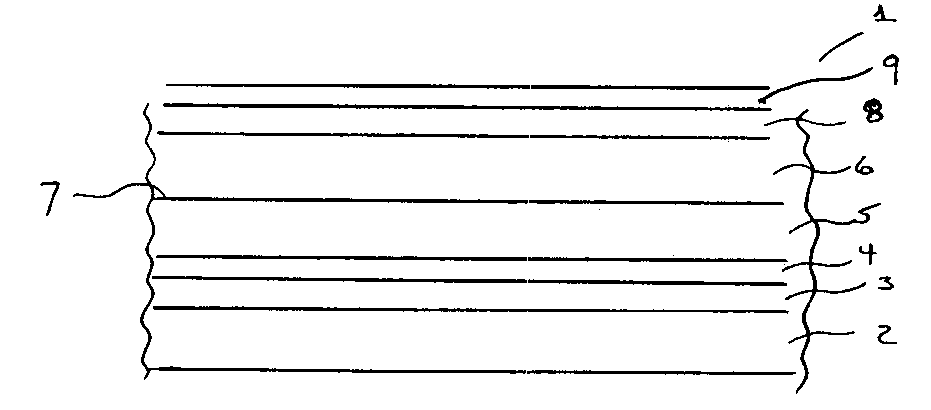
[0032] Thin film photovoltaic devices were made as follows and tested for efficiency in converting light energy to electrical energy. The photovoltaic devices tested had a 3 mm thick float glass sheet as a substrate material. The substrate was coated with a layer of transparent conducting tin oxide about 0.5 to 0.6 microns thick. The conductive tin oxide was applied using chemical vapor deposition and had a resistivity of about 1×10⁻⁴ ohm.cm. A second transparent layer of tin and zinc oxide in a molar ratio of 99 to 1 was deposited on the first transparent layer using reactive DC magnetic sputtering in an oxygen atmosphere at a pressure of about 1 millitorr. The thickness of the second transparent layer was varied as shown in the Table 1. After deposition, the second transparent layer was heated in air at a temperature of 500° C. for 20 minutes. The second transparent layers had resistivities that were about the same. A 0.05 microns film of cadmium sulfide was deposited on the secon...


PUM

PropertyMeasurementUnit
thicknessaaaaaaaaaa
thicknessaaaaaaaaaa
resistivityaaaaaaaaaa

Abstract

This invention is a layered thin film semiconductor device comprising a first transparent layer; a thin, second transparent layer having a conductivity less than the first transparent layer; an n-type layer; and a p-type layer comprising one or more IIB and VIA elements. This invention is also a method for making such semiconductor device. The thin film semiconductor devices of this invention are useful for making photovoltaic devices.

Description

FIELD OF THE INVENTION [0001] This application claims the benefit of Provisional Patent Application No. 60 / 289,481, filed on May 8, 2001.[0002] This invention relates to a new, thin film semiconductor device. More particularly, this invention relates to a new thin film photovoltaic semiconductor device having improved efficiency in converting solar or other light energy into electrical energy. This invention also relates to a method of manufacturing such semiconductor and photovoltaic device. BACKGROUND OF THE INVENTION [0003] Solar power is an important source of renewable electrical energy. The continuous challenge in the field of solar energy is to develop and manufacture photovoltaic devices having a high efficiency for converting sunlight into electrical energy. The more efficient the photovoltaic device is at performing such a conversion, the greater amount of electricity can be generated for a given investment. While a number of different types of photovoltaic devices have be...

Claims


Application Information

Patent Timeline
Patent Type & Authority Applications(United States)
IPC IPC(8): H01L21/00H01L29/22H01L31/00H01L31/0224H01L31/073
CPCH01L31/02168H01L31/022466H01L31/0296H01L31/073Y02E10/543Y02E10/52H01L31/056
Inventor CUNNINGHAM, DANIEL W.RUBCICH, MARC P.
Owner BP CORP NORTH AMERICA INC
Why Eureka
Try Eureka